
Datasheet
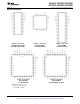
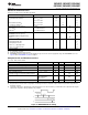

PDIP
PDIP
LQFP
PDIP
COP8SGE5, COP8SGE7, COP8SGH5
COP8SGK5, COP8SGR5, COP8SGR7
www.ti.com
SNOS516E –JANUARY 2000–REVISED APRIL 2013
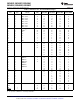
Ordering Information
Figure 7. Part Numbering Scheme
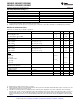
Electrical Characteristics
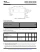
Absolute Maximum Ratings
(1)(2)
Supply Voltage (V
CC
) 7V
Voltage at Any Pin −0.3V to V
CC
+0.3V
Total Current into V
CC
Pin (Source) 100 mA
Total Current out of GND Pin (Sink) 110 mA
Storage Temperature Range −65°C to +140°C
ESD Protection Level 2kV (Human Body Model)
(1) Absolute maximum ratings indicate limits beyond which damage to the device may occur. DC and AC electrical specifications are not
ensured when operating the device at absolute maximum ratings.
(2) If Military/Aerospace specified devices are required, please contact the TI Sales Office/ Distributors for availability and specifications.
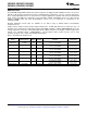
DC Electrical Characteristics
−40°C ≤ T
A
≤ +85°C unless otherwise specified.
Parameter Conditions Min Typ Max Units
Operating Voltage 2.7 5.5 V
Power Supply Rise Time 10 50 x 10
6
ns
V
CC
Start Voltage to Ensure POR 0 0.25 V
Power Supply Ripple
(1)
Peak-to-Peak 0.1 V
cc
V
Supply Current
(2)
CKI = 15 MHz V
CC
= 5.5V, t
C
= 0.67 μs 9.0 mA
CKI = 10 MHz V
CC
= 5.5V, t
C
= 1 μs 6.0 mA
CKI = 4 MHz V
CC
= 4.5V, t
C
= 2.5 μs 2.1 mA
HALT Current
(3)
V
CC
= 5.5V, CKI = 0 MHz <4 10 μA
(1) Maximum rate of voltage change must be < 0.5 V/ms.
(2) Supply and IDLE currents are measured with CKI driven with a square wave Oscillator, External Oscillator, inputs connected to V
CC
and
outputs driven low but not connected to a load.
(3) The HALT mode will stop CKI from oscillating in the R/C and the Crystal configurations. In the R/C configuration, CKI is forced high
internally. In the crystal or external configuration, CKI is TRI-STATE. Measurement of I
DD
HALT is done with device neither sourcing nor
sinking current; with L. F, C, G0, and G2–G5 programmed as low outputs and not driving a load; all outputs programmed low and not
driving a load; all inputs tied to V
CC
; clock monitor disabled. Parameter refers to HALT mode entered via setting bit 7 of the G Port data
register.
Copyright © 2000–2013, Texas Instruments Incorporated Submit Documentation Feedback 7
Product Folder Links: COP8SGE5 COP8SGE7 COP8SGH5 COP8SGK5 COP8SGR5 COP8SGR7