
Datasheet
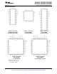

COP8SGE5, COP8SGE7, COP8SGH5
COP8SGK5, COP8SGR5, COP8SGR7
SNOS516E –JANUARY 2000–REVISED APRIL 2013
www.ti.com
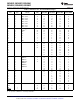
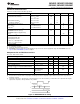
DC Electrical Characteristics (continued)
−40°C ≤ T
A
≤ +85°C unless otherwise specified.
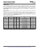
Parameter Conditions Min Typ Max Units
IDLE Current
(2)
CKI = 15 MHz V
CC
= 5.5V, t
C
= 0.67 μs 2.25 mA
CKI = 10 MHz V
CC
= 5.5V, t
C
= 1 μs 1.5 mA
CKI = 4 MHz V
CC
= 4.5V, t
C
= 2.5 μs 0.8 mA
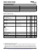
Input Levels (V
IH
, V
IL
)
RESET
0.8 V
cc
Logic High V
Logic Low 0.2 V
cc
V
CKI, All Other Inputs
Logic High 0.7 V
cc
V
Logic Low 0.2 V
cc
V
Internal Bias Resistor for the 0.5 1 2 MΩ
Crystal/Resonator Oscillator
CKI Resistance to V
CC
or GND when R/C V
CC
= 5.5V 5 8 11 kΩ
Oscillator is selected
Hi-Z Input Leakage V
CC
= 5.5V −2 +2 μA
Input Pullup Current V
CC
= 5.5V, V
IN
= 0V −40 −250 μA
G and L Port Input Hysteresis V
CC
= 5.5V 0.25 V
cc
V
Output Current Levels
D Outputs
Source V
CC
= 4.5V, V
OH
= 3.3V −0.4 mA
V
CC
= 2.7V, V
OH
= 1.8V -0.2 mA
Sink V
CC
= 4.5V, V
OL
= 1.0V 10 mA
V
CC
= 2.7V, V
OL
= 0.4V 2 mA
All Others
Source (Weak Pull-Up Mode) V
CC
= 4.5V, V
OH
= 2.7V −10.0 −110 μA
V
CC
= 2.7V, V
OH
= 1.8V -2.5 -33 μA
Source (Push-Pull Mode) V
CC
= 4.5V, V
OH
= 3.3V −0.4 mA
V
CC
= 2.7V, V
OH
= 1.8V -0.2 mA
Sink (Push-Pull Mode) V
CC
= 4.5V, V
OL
= 0.4V 1.6 mA
V
CC
= 2.7V, V
OL
= 0.4V 0.7 mA
TRI-STATE Leakage V
CC
= 5.5V −2 +2 μA
Allowable Sink Current per Pin
(4)
D Outputs and L0 to L3 15 mA
All Others 3 mA
Maximum Input Current without Latchup
(5)
Room Temp. ±200 mA
RAM Retention Voltage, Vr 2.0 V
V
CC
Rise Time from a V
CC
≥ 2.0V See
(6)
12 μs
EPROM Data Retenton
(7)
,
(4)
T
A
= 55°C >29 years
Input Capacitance See
(4)
7 pF
Load Capacitance on D2 See
(4)
1000 pF
(4) Parameter characterized but not tested.
(5) Pins G6 and RESET are designed with a high voltage input network. These pins allow input voltages > V
CC
and the pins will have sink
current to V
CC
when biased at voltages > V
CC
(the pins do not have source current when biased at a voltage below V
CC
). The effective
resistance to V
CC
is 750Ω (typical). These two pins will not latch up. The voltage at the pins must be limited to < 14V. WARNING:
Voltages in excess of 14V will cause damage to the pins. This warning excludes ESD transients.
(6) Rise times faster than the minimum specification may trigger an internal power-on-reset.
(7) TI uses the High Temperature Storage Life (HTSL) test to evaluate the data retention capabilities of the EPROM memory cells used in
our OTP microcontrollers. Qualification devices have been stressed at 150°C for 1000 hours. Under these conditions, our EPROM cells
exhibit data retention capabilities in excess of 29 years. This is based on an activation energy of 0.7eV derated to 55°C.
8 Submit Documentation Feedback Copyright © 2000–2013, Texas Instruments Incorporated
Product Folder Links: COP8SGE5 COP8SGE7 COP8SGH5 COP8SGK5 COP8SGR5 COP8SGR7