
Datasheet

COP8SGE5, COP8SGE7, COP8SGH5
COP8SGK5, COP8SGR5, COP8SGR7
www.ti.com
SNOS516E –JANUARY 2000–REVISED APRIL 2013
Since G6 is an input only pin and G7 is the dedicated CKO clock output pin (crystal clock option) or general
purpose input (R/C or external clock option), the associated bits in the data and configuration registers for G6
and G7 are used for special purpose functions as outlined below. Reading the G6 and G7 data bits will return
zeroes.
Each device will be placed in the HALT mode by writing a “1” to bit 7 of the Port G Data Register. Similarly the
device will be placed in the IDLE mode by writing a “1” to bit 6 of the Port G Data Register.
Writing a “1” to bit 6 of the Port G Configuration Register enables the MICROWIRE/PLUS to operate with the
alternate phase of the SK clock. The G7 configuration bit, if set high, enables the clock start up delay after HALT
when the R/C clock configuration is used.
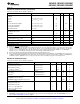
Config. Reg. Data Reg.
G7 CLKDLY HALT
G6 Alternate SK IDLE
Port G has the following alternate features:
G7 CKO Oscillator dedicated output or general purpose input
G6 SI (MICROWIRE Serial Data Input)
G5 SK (MICROWIRE Serial Clock)
G4 SO (MICROWIRE Serial Data Output)
G3 T1A (Timer T1 I/O)
G2 T1B (Timer T1 Capture Input)
G1 WDOUT WATCHDOG and/or CLock Monitor if WATCHDOG enabled, otherwise it is a general purpose
I/O
G0 INTR (External Interrupt Input)
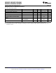
Port C is an 8-bit I/O port. The 40-pin device does not have a full complement of Port C pins. The unavailable
pins are not terminated. A read operation on these unterminated pins will return unpredictable values. The 28 pin
device do not offer Port C. On this device, the associated Port C Data and Configuration registers should not be
used.
Port F is an 8-bit I/O port. The 28--pin device does not have a full complement of Port F pins. The unavailable
pins are not terminated. A read operation on these unterminated pins will return unpredictable values.
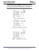
Port F1–F3 are used for Comparator 1. Port F4–F6 are used for Comparator 2.
The Port F has the following alternate features:
F6 COMP2OUT (Comparator 2 Output)
F5 COMP2+IN (Comparator 2 Positive Input)
F4 COMP2-IN (Comparator 2 Negative Input)
F3 COMP1OUT (Comparator 1 Output)
F2 COMP1+IN (Comparator 1 Positive Input)
F1 COMP1-IN (Comparator 1 Negative Input)
NOTE
For compatibility with existing software written for COP888xG devices and with existing
Mask ROM devices, a read of the Port I input pins (address xxD7) will return the same
data as reading the Port F input pins (address xx96). It is recommended new applications
which will go to production with the COP8SGx use the Port F addresses. Note that
compatible ROM devices contains the input only Port I instead of the bi-directional Port F.
Port D is an 8-bit output port that is preset high when RESET goes low. The user can tie two or more D port
outputs (except D2) together in order to get a higher drive.
Copyright © 2000–2013, Texas Instruments Incorporated Submit Documentation Feedback 15
Product Folder Links: COP8SGE5 COP8SGE7 COP8SGH5 COP8SGK5 COP8SGR5 COP8SGR7