
Datasheet

COP8SGE5, COP8SGE7, COP8SGH5
COP8SGK5, COP8SGR5, COP8SGR7
www.ti.com
SNOS516E –JANUARY 2000–REVISED APRIL 2013
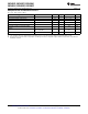
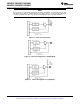
The 128 bytes of RAM contained in the base segment are split between the lower and upper base segments.
The first 112 bytes of RAM are resident from address 0000 to 006F in the lower base segment, while the
remaining 16 bytes of RAM represent the 16 data memory registers located at addresses 00F0 to 00FF of the
upper base segment. No RAM is located at the upper sixteen addresses (0070 to 007F) of the lower base
segment.
Additional RAM beyond these initial 128 bytes, however, will always be memory mapped in groups of 128 bytes
(or less) at the data segment address extensions (XX00 to XX7F) of the lower base segment. The additional 384
bytes of RAM in this device are memory mapped at address locations 0100 to 017F, 0200 to 027F and 0300 to
037F hex.
Memory address ranges 0200 to 027F and 0300 to 037F are unavailable on the COP8SGx5 and, if read, will
return underfined data.
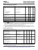
ECON (CONFIGURATION) REGISTER
For compatibility with COP8SGx7 devices, mask options are defined by an ECON Configuration Register which
is programmed at the same time as the program code. Therefore, the register is programmed at the same time
as the program memory.
The format of the ECON register is as follows:
Bit 7 Bit 6 Bit 5 Bit 4 Bit 3 Bit 2 Bit 1 Bit 0
X POR SECURITY CKI 2 CKI 1 WATCH F-Port HALT
DOG
Bit 7 = xThis is for factory test. The polarity is “Don't Care.”
Bit 6 = 1Power-on reset enabled.
= 0Power-on reset disabled.
Bit 5 = 1Security enabled.
Bits 4, 3 = 0, 0External CKI option selected. G7 is available as a HALT restart and/or general purpose input. CKI
is clock input.
= 0, 1R/C oscillator option selected. G7 is available as a HALT restart and/or general purpose input.
CKI clock input. Internal R/C components are supplied for maximum R/C frequency.
= 1, 0Crystal oscillator with on-chip crystal bias resistor disabled. G7 (CKO) is the clock generator
output to crystal/resonator.
= 1, 1Crystal oscillator with on-chip crystal bias resistor enabled. G7 (CKO) is the clock generator
output to crystal/resonator.
Bit 2 = 1WATCHDOG feature disabled. G1 is a general purpose I/O.
= 0WATCHDOG feature enabled. G1 pin is WATCHDOG output with weak pullup.
Bit 1 = 1Force port I compatibility. Disable port F outputs and pull-ups. This is intended for compatibility with
existing code and Mask ROMMed devices only. This bit should be programmed to 0 for all other
applications.
= 0Enable full port F capability.
Bit 0 = 1HALT mode disabled.
= 0HALT mode enabled.
USER STORAGE SPACE IN EPROM
The ECON register is outside of the normal address range of the ROM and can not be accessed by the
executing software.
The COP8 assembler defines a special ROM section type, CONF, into which the ECON may be coded. Both
ECON and User Data are programmed automatically by programmers that are certified by TI.
Copyright © 2000–2013, Texas Instruments Incorporated Submit Documentation Feedback 19
Product Folder Links: COP8SGE5 COP8SGE7 COP8SGH5 COP8SGK5 COP8SGR5 COP8SGR7