
Datasheet

COP8SGE5, COP8SGE7, COP8SGH5
COP8SGK5, COP8SGR5, COP8SGR7
www.ti.com
SNOS516E –JANUARY 2000–REVISED APRIL 2013
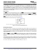
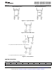
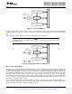
Figure 24. Timer in PWM Mode
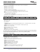
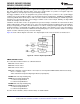
In this mode the input pin TxB can be used as an independent positive edge sensitive interrupt input if the
TxENB control flag is set. The occurrence of a positive edge on the TxB input pin is latched into the TxPNDB
flag.
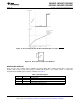
Figure 25 shows a block diagram of the timer in External Event Counter mode.
NOTE
The PWM output is not available in this mode since the TxA pin is being used as the
counter input clock.
Figure 25. Timer in External Event Counter Mode
Mode 3. Input Capture Mode
Each device can precisely measure external frequencies or time external events by placing the timer block, Tx, in
the input capture mode. In this mode, the reload registers serve as independent capture registers, capturing the
contents of the timer when an external event occurs (transition on the timer input pin). The capture registers can
be read while maintaining count, a feature that lets the user measure elapsed time and time between events. By
saving the timer value when the external event occurs, the time of the external event is recorded. Most
microcontrollers have a latency time because they cannot determine the timer value when the external event
occurs. The capture register eliminates the latency time, thereby allowing the applications program to retrieve the
timer value stored in the capture register.
In this mode, the timer Tx is constantly running at the fixed t
C
rate. The two registers, RxA and RxB, act as
capture registers. Each register acts in conjunction with a pin. The register RxA acts in conjunction with the TxA
pin and the register RxB acts in conjunction with the TxB pin.
Copyright © 2000–2013, Texas Instruments Incorporated Submit Documentation Feedback 29
Product Folder Links: COP8SGE5 COP8SGE7 COP8SGH5 COP8SGK5 COP8SGR5 COP8SGR7