
Datasheet


CY29FCT520T
MULTILEVEL PIPELINE REGISTER
WITH 3-STATE OUTPUTS
SCCS011C – MAY 1994 – REVISED NOVEMBER 2001
1
POST OFFICE BOX 655303 • DALLAS, TEXAS 75265
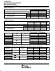
Function, Pinout, and Drive Compatible
With FCT, F Logic, and AM29520
Reduced V
OH
(Typically = 3.3 V) Version of
Equivalent FCT Functions
Edge-Rate Control Circuitry for
Significantly Improved Noise
Characteristics
I
off
Supports Partial-Power-Down Mode
Operation
Matched Rise and Fall Times
Fully Compatible With TTL Input and
Output Logic Levels
ESD Protection Exceeds JESD 22
– 2000-V Human-Body Model (A114-A)
– 200-V Machine Model (A115-A)
– 1000-V Charged-Device Model (C101)
Single- and Dual-Pipeline Operation Modes
Multiplexed Data Inputs and Outputs
CY29FCT520T
– 64-mA Output Sink Current
32-mA Output Source Current
CY29FCT520ATDMB, CY29FCT520BTDMB
– 32-mA Output Sink Current
12-mA Output Source Current
3-State Outputs
description
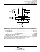
The CY29FCT520T is a multilevel 8-bit-wide pipeline register. The device consists of four registers, A1, A2, B1,
and B2, which are configured by the instruction inputs I
0
, I
1
as a single four-level pipeline or as two two-level
pipelines. The contents of any register can be read at the multiplexed output at any time by using the
multiplex-selection controls (S
0
and S
1
).
The pipeline registers are positive-edge triggered, and data is shifted by the rising edge of the clock input.
Instruction I = 0 selects the four-level pipeline mode. Instruction I = 1 selects the two-level B pipeline, while I = 2
selects the two-level A pipeline. I = 3 is the hold instruction; no shifting is performed by the clock in this mode.
In the two-level operation mode, data is shifted from level 1 to level 2 and new data is loaded into level 1.
This device is fully specified for partial-power-down applications using I
off
. The I
off
circuitry disables the outputs,
preventing damaging current backflow through the device when it is powered down.
Copyright 2001, Texas Instruments Incorporated
PRODUCTION DATA information is current as of publication date.
Products conform to specifications per the terms of Texas Instruments
standard warranty. Production processing does not necessarily include
testing of all parameters.
Please be aware that an important notice concerning availability, standard warranty, and use in critical applications of
Texas Instruments semiconductor products and disclaimers thereto appears at the end of this data sheet.
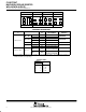
I
0
I
1
D
0
D
1
D
2
D
3
D
4
D
5
D
6
D
7
CLK
GND
D, P, OR SO PACKAGE
(TOP VIEW)
1
2
3
4
5
6
7
8
9
10
11
12
24
23
22
21
20
19
18
17
16
15
14
13
V
CC
S
0
S
1
Y
0
Y
1
Y
2
Y
3
Y
4
Y
5
Y
6
Y
7
OE
On products compliant to MIL-PRF-38535, all parameters are tested
unless otherwise noted. On all other products, production
processing does not necessarily include testing of all parameters.