
Datasheet


CY74FCT2574T
8-BIT REGISTER
WITH 3-STATE OUTPUTS
SCCS076 – OCTOBER 2001
1
POST OFFICE BOX 655303 • DALLAS, TEXAS 75265
Function and Pinout Compatible With FCT
and F Logic
25-Ω Output Series Resistors to Reduce
Transmission-Line Reflection Noise
Reduced V
OH
(Typically = 3.3 V) Version of
Equivalent FCT Functions
Edge-Rate Control Circuitry for
Significantly Improved Noise
Characteristics
I
off
Supports Partial-Power-Down Mode
Operation
Matched Rise and Fall Times
Fully Compatible With TTL Input and
Output Logic Levels
ESD Protection Exceeds JESD 22
– 2000-V Human-Body Model (A114-A)
– 200-V Machine Model (A115-A)
– 1000-V Charged-Device Model (C101)
3-State Outputs
12-mA Output Sink Current
15-mA Output Source Current
Edge-Triggered D-Type Inputs
250-MHz Typical Switching Rate
description
The CY74FCT2574T is a high-speed, low-power, octal D-type flip-flop featuring separate D-type inputs for each
flip-flop. On-chip termination resistors at the outputs reduce system noise caused by reflections. The
CY74FCT2574T can replace the CY74FCT574T to reduce noise in an existing design. This device has 3-state
outputs for bus-oriented applications. A buffered clock (CP) and output-enable (OE
) inputs are common to all
flip-flops. The CY74FCT2574T is identical to the CY74FCT2374T, except that on the CY74FCT2574T all
outputs are on one side of the package and all inputs are on the other side. The flip-flops in the CY74FCT2574T
store the state of their individual D inputs that meet the setup-time and hold-time requirements on the low-to-high
CP transition. When OE
is low, the contents of the flip-flops are available at the outputs. When OE is high, the
outputs are in the high-impedance state. The state of OE
does not affect the state of the flip-flops.
This device is fully specified for partial-power-down applications using I
off
. The I
off
circuitry disables the outputs,
preventing damaging current backflow through the device when it is powered down.
Copyright 2001, Texas Instruments Incorporated
PRODUCTION DATA information is current as of publication date.
Products conform to specifications per the terms of Texas Instruments
standard warranty. Production processing does not necessarily include
testing of all parameters.
Please be aware that an important notice concerning availability, standard warranty, and use in critical applications of
Texas Instruments semiconductor products and disclaimers thereto appears at the end of this data sheet.
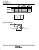
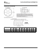
1
2
3
4
5
6
7
8
9
10
20
19
18
17
16
15
14
13
12
11
OE
D
0
D
1
D
2
D
3
D
4
D
5
D
6
D
7
GND
V
CC
O
0
O
1
O
2
O
3
O
4
O
5
O
6
O
7
CP
Q OR SO PACKAGE
(TOP VIEW)