
Datasheet
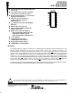


CY74FCT2574T
8-BIT REGISTER
WITH 3-STATE OUTPUTS
SCCS076 – OCTOBER 2001
4
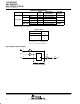
POST OFFICE BOX 655303 • DALLAS, TEXAS 75265
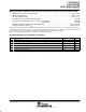
electrical characteristics over recommended operating free-air temperature range (unless
otherwise noted)
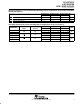
PARAMETER TEST CONDITIONS MIN TYP
†
MAX UNIT
V
IK
V
CC
= 4.75 V, I
IN
= –18 mA –0.7 –1.2 V
V
OH
V
CC
= 4.75 V, I
OH
= –15 mA 2.4 3.3 V
V
OL
V
CC
= 4.75 V, I
OL
= 12 mA 0.3 0.55 V
R
OUT
V
CC
= 4.75 V, I
OL
= 12 mA 20 25 40 Ω
V
hys
All inputs 0.2 V
I
I
V
CC
= 5.25 V, V
IN
= V
CC
5 µA
I
IH
V
CC
= 5.25 V, V
IN
= 2.7 V ±1 µA
I
IL
V
CC
= 5.25 V, V
IN
= 0.5 V ±1 µA
I
OZH
V
CC
= 5.25 V, V
OUT
= 2.7 V 10 µA
I
OZL
V
CC
= 5.25 V, V
OUT
= 0.5 V –10 µA
I
OS
‡
V
CC
= 5.25 V, V
OUT
= 0 V –60 –120 –225 mA
I
off
V
CC
= 0 V, V
OUT
= 4.5 V ±1 µA
I
CC
V
CC
= 5.25 V, V
IN
≤ 0.2 V, V
IN
≥ V
CC
– 0.2 V 0.1 0.2 mA
∆I
CC
V
CC
= 5.25 V, V
IN
= 3.4 V
§
, f
1
= 0, Outputs open 0.5 2 mA
I
CCD
¶
V
CC
= 5.25 V, Outputs open, One input switching at 50% duty cycle,
OE
= GND, V
IN
≤ 0.2 V or V
IN
≥ V
CC
– 0.2 V
0.06 0.12
mA/
MHz
#
V
CC
= 5 25 V
One bit switching
at f
1
= 5 MHz
V
IN
≤ 0.2 V or
V
IN
≥ V
CC
– 0.2V
0.7 1.4
I
C
#
V
CC
=
5
.
25
V
,
Outputs open,
1
at 50% duty cycle
V
IN
= 3.4 V or GND 1.2 3.4
mA
I
C
#
,
f
0
= 10 MHz,
OE
= GND
Eight bits switching
at f
1
= 2.5 MHz
V
IN
≤ 0.2 V or
V
IN
≥ V
CC
– 0.2 V
1.6 3.2
||
mA
1
at 50% duty cycle
V
IN
= 3.4 V or GND 3.9 12.2
||
C
i
5 10 pF
C
o
9 12 pF
†
Typical values are at V
CC
= 5 V, T
A
= 25°C.
‡
Not more than one output should be shorted at a time. Duration of short should not exceed one second. The use of high-speed test apparatus
and/or sample-and-hold techniques are preferable to minimize internal chip heating and more accurately reflect operational values. Otherwise,
prolonged shorting of a high output can raise the chip temperature well above normal and cause invalid readings in other parametric tests. In
any sequence of parameter tests, I
OS
tests should be performed last.
§
Per TTL-driven input (V
IN
= 3.4 V); all other inputs at V
CC
or GND
¶
This parameter is derived for use in total power-supply calculations.
#
I
C
= I
CC
+ ∆I
CC
× D
H
× N
T
+ I
CCD
(f
0
/2 + f
1
× N
1
)
Where:
I
C
= Total supply current
I
CC
= Power-supply current with CMOS input levels
∆I
CC
= Power-supply current for a TTL high input (V
IN
= 3.4 V)
D
H
= Duty cycle for TTL inputs high
N
T
= Number of TTL inputs at D
H
I
CCD
= Dynamic current caused by an input transition pair (HLH or LHL)
f
0
= Clock frequency for registered devices, otherwise zero
f
1
= Input signal frequency
N
1
= Number of inputs changing at f
1
All currents are in milliamperes and all frequencies are in megahertz.
||
Values for these conditions are examples of the I
CC
formula.