
Datasheet


CY74FCT2574T
8-BIT REGISTER
WITH 3-STATE OUTPUTS
SCCS076 – OCTOBER 2001
6
POST OFFICE BOX 655303 • DALLAS, TEXAS 75265
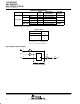
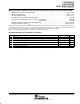
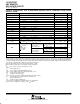
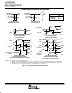
PARAMETER MEASUREMENT INFORMATION
3 V
3 V
0 V
0 V
t
h
t
su
VOLTAGE WAVEFORMS
SETUP AND HOLD TIMES
Data Input
t
PLH
t
PHL
t
PHL
t
PLH
V
OH
V
OH
V
OL
V
OL
3 V
0 V
Input
Out-of-Phase
Output
In-Phase
Output
Timing Input
VOLTAGE WAVEFORMS
PROPAGATION DELAY TIMES
INVERTING AND NONINVERTING OUTPUTS
Output
Control
Output
Waveform 1
(see Note B)
Output
Waveform 2
(see Note B)
V
OL
V
OH
t
PZL
t
PZH
t
PLZ
t
PHZ
≈3.5 V
0 V
V
OL
+ 0.3 V
≈0 V
3 V
VOLTAGE WAVEFORMS
ENABLE AND DISABLE TIMES
LOW- AND HIGH-LEVEL ENABLING
t
PLH
/t
PHL
t
PLZ
/t
PZL
t
PHZ
/t
PZH
Open
7 V
Open
TEST S1
3 V
0 V
t
w
VOLTAGE WAVEFORMS
PULSE DURATION
Input
NOTES: A. C
L
includes probe and jig capacitance.
B. Waveform 1 is for an output with internal conditions such that the output is low except when disabled by the output control.
Waveform 2 is for an output with internal conditions such that the output is high except when disabled by the output control.
C. The outputs are measured one at a time with one input transition per measurement.
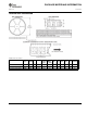
From Output
Under Test
C
L
= 50 pF
(see Note A)
LOAD CIRCUIT FOR
3-STATE OUTPUTS
S1
7 V
500 Ω
GND
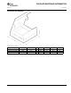
From Output
Under Test
C
L
= 50 pF
(see Note A)
Test
Point
LOAD CIRCUIT FOR
TOTEM-POLE OUTPUTS
Open
V
OH
– 0.3 V
500 Ω
500 Ω
1.5 V1.5 V
1.5 V 1.5 V
1.5 V 1.5 V
1.5 V 1.5 V
1.5 V
1.5 V1.5 V
1.5 V 1.5 V
1.5 V
1.5 V
Figure 1. Load Circuit and Voltage Waveforms