
Datasheet
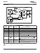
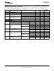

V
A
V
OUTA
V
OUTB
NC
NC
SCLK
D
IN
V
REFIN
GND
SON
1
2
3
4
5
10
9
8
7
6
SYNC
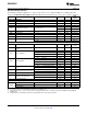
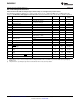
V
A
V
OUTA
V
OUTB
NC
NC
SCLK
D
IN
V
REFIN
GND
VSSOP
1
2
3
4
5
10
9
8
7
6
SYNC
DAC082S085
www.ti.com
SNAS365F –MAY 2006–REVISED MARCH 2013
DAC082S085 8-Bit Micro Power DUAL Digital-to-Analog Converter with Rail-to-Rail Output
Check for Samples: DAC082S085
1
FEATURES
DESCRIPTION
The DAC082S085 is a full-featured, general purpose
23
• Ensured Monotonicity
DUAL 8-bit voltage-output digital-to-analog converter
• Low Power Operation
(DAC) that can operate from a single +2.7V to 5.5V
• Rail-to-Rail Voltage Output
supply and consumes 0.6 mW at 3V and 1.6 mW at
5V. The DAC082S085 is packaged in 10-lead SON
• Power-on Reset to 0V
and VSSOP packages. The 10-lead SON package
• Simultaneous Output Updating
makes the DAC082S085 the smallest DUAL DAC in
• Wide power supply range (+2.7V to +5.5V)
its class. The on-chip output amplifier allows rail-to-
rail output swing and the three wire serial interface
• Industry's Smallest Package
operates at clock rates up to 40 MHz over the entire
• Power Down Modes
supply voltage range. Competitive devices are limited
to 25 MHz clock rates at supply voltages in the 2.7V
APPLICATIONS
to 3.6V range. The serial interface is compatible with
standard SPI™, QSPI, MICROWIRE and DSP
• Battery-Powered Instruments
interfaces.
• Digital Gain and Offset Adjustment
The reference for the DAC082S085 serves both
• Programmable Voltage & Current Sources
channels and can vary in voltage between 1V and V
A
,
• Programmable Attenuators
providing the widest possible output dynamic range.
The DAC082S085 has a 16-bit input shift register that
KEY SPECIFICATIONS
controls the outputs to be updated, the mode of
operation, the powerdown condition, and the binary
• Resolution: 8 Bits
input data. Both outputs can be updated
• INL: ±0.5 LSB (Max)
simultaneously or individually depending on the
• DNL: +0.18 / -0.13 LSB (Max)
setting of the two mode of operation bits.
• Settling Time: 4.5 µs (Max)
A power-on reset circuit ensures that the DAC output
• Zero Code Error: +15mV (Max)
powers up to zero volts and remains there until there
is a valid write to the device. A power-down feature
• Full-Scale error: -0.75% FS (Max)
reduces power consumption to less than a microWatt
• Supply Power
with three different termination options.
– Normal: 0.6mW (3V) / 1.6 mW (5V) (Typ)
The low power consumption and small packages of
– Power Down: 0.3 µW (3V) / 0.8 µW (5V)
the DAC082S085 make it an excellent choice for use
(Typ)
in battery operated equipment.
The DAC082S085 is one of a family of pin compatible
DACs, including the 10-bit DAC102S085 and the 12-
bit DAC124S085. The DAC082S085 operates over
the extended industrial temperature range of −40°C
to +105°C.
Pin Configuration
1
Please be aware that an important notice concerning availability, standard warranty, and use in critical applications of
Texas Instruments semiconductor products and disclaimers thereto appears at the end of this data sheet.
2SPI is a trademark of Motorola, Inc..
3All other trademarks are the property of their respective owners.
PRODUCTION DATA information is current as of publication date.
Copyright © 2006–2013, Texas Instruments Incorporated
Products conform to specifications per the terms of the Texas
Instruments standard warranty. Production processing does not
necessarily include testing of all parameters.