
Datasheet


D
IN
SCLK
V
A
GND
V
OUT
1
2
3
6
5
4
SYNC
1
2
3
4
8
7
6
5
GND
D
IN
SCLK
V
A
NC
NC
V
OUT
SYNC
DAC101S101, DAC101S101-Q1
www.ti.com
SNAS321F –JUNE 2005–REVISED MARCH 2013
DAC101S101/DAC101S101Q 10-Bit Micro Power, RRO Digital-to-Analog Converter
Check for Samples: DAC101S101, DAC101S101-Q1
1
FEATURES
DESCRIPTION
The DAC101S101 is a full-featured, general purpose
2
• DAC101S101Q is AEC-Q100 Grade 1 Qualified
10-bit voltage-output digital-to-analog converter
and is Manufactured on an Automotive Grade
(DAC) that can operate from a single +2.7V to 5.5V
Flow.
supply and consumes just 175 µA of current at 3.6
• Ensured Monotonicity
Volts. The on-chip output amplifier allows rail-to-rail
output swing and the three wire serial interface
• Low Power Operation
operates at clock rates up to 30 MHz over the
• Rail-to-Rail Voltage Output
specified supply voltage range and is compatible with
• Power-on Reset to Zero Volts Output
standard SPI, QSPI, MICROWIRE and DSP
• Wide Temperature Range of −40°C to +125°C
interfaces. Competitive devices are limited to 20 MHz
clock rates at supply voltages in the 2.7V to 3.6V
• Wide Power Supply Range of +2.7V to +5.5V
range.
• Small Packages
The supply voltage for the DAC101S101 serves as its
• Power Down Feature
voltage reference, providing the widest possible
output dynamic range. A power-on reset circuit
APPLICATIONS
ensures that the DAC output powers up to zero volts
and remains there until there is a valid write to the
• Battery-Powered Instruments
device. A power-down feature reduces power
• Digital Gain and Offset Adjustment
consumption to less than a microWatt.
• Programmable Voltage & Current Sources
The low power consumption and small packages of
• Programmable Attenuators
the DAC101S101 make it an excellent choice for use
• Automotive
in battery operated equipment.
The DAC101S101 is a direct replacement for the
KEY SPECIFICATIONS
AD5310 and is one of a family of pin compatible
• Resolution 10 bits
DACs, including the 8-bit DAC081S101 and the 12-bit
DAC121S101. The DAC101S101 operates over the
• DNL +0.15, -0.05 LSB (typ)
extended industrial temperature range of −40°C to
• Output Settling Time 8 μs (typ)
+105°C while the DAC101S101Q operates over the
• Zero Code Error 3.3 mV (typ)
Grade 1 automotive temperature range of −40°C to
+125°C. The DAC101S101 is available in a 6-lead
• Full-Scale Error −0.06 %FS (typ)
SOT and an 8-lead VSSOP and the DAC101S101Q
• Power Consumption
is availabe in the 6-lead SOT only.
– Normal Mode, 0.63 mW (3.6V) / 1.41 mW
(5.5V) typ
– Pwr Down Mode, 0.14 μW (3.6V) / 0.33 μW
(5.5V) typ
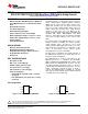
Pin Configuration
Figure 1. Package Number DDC0006A Figure 2. Package Number DGK0008A
1
Please be aware that an important notice concerning availability, standard warranty, and use in critical applications of
Texas Instruments semiconductor products and disclaimers thereto appears at the end of this data sheet.
2All trademarks are the property of their respective owners.
PRODUCTION DATA information is current as of publication date.
Copyright © 2005–2013, Texas Instruments Incorporated
Products conform to specifications per the terms of the Texas
Instruments standard warranty. Production processing does not
necessarily include testing of all parameters.