
Datasheet

DAC128S085
www.ti.com
SNAS407F –AUGUST 2007–REVISED MARCH 2013
DAC128S085 12-Bit Micro Power OCTAL Digital-to-Analog Converter with Rail-to-Rail
Outputs
Check for Samples: DAC128S085
1
FEATURES
DESCRIPTION
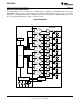
The DAC128S085 is a full-featured, general purpose
23
• Guaranteed Monotonicity
OCTAL 12-bit voltage-output digital-to-analog
• Low Power Operation
converter (DAC) that can operate from a single +2.7V
• Rail-to-Rail Voltage Output
to +5.5V supply and consumes 1.95 mW at 3V and
4.85 mW at 5V. The DAC128S085 is packaged in a
• Daisy Chain Capability
16-lead WQFN package and a 16-lead TSSOP
• Power-on Reset to 0V
package. The WQFN package makes the
• Simultaneous Output Updating
DAC128S085 the smallest OCTAL DAC in its class.
The on-chip output amplifiers allow rail-to-rail output
• Individual Channel Power Down Capability
swing and the three wire serial interface operates at
• Wide power supply range (+2.7V to +5.5V)
clock rates up to 40 MHz over the entire supply
• Dual Reference Voltages with range of 0.5V to
voltage range. Competitive devices are limited to 25
V
A MHz clock rates at supply voltages in the 2.7V to
3.6V range. The serial interface is compatible with
• Operating Temperature Range of −40°C to
standard SPI™, QSPI, MICROWIRE and DSP
+125°C
interfaces. The DAC128S085 also offers daisy chain
• Industry's Smallest Package
operation where an unlimited number of
DAC128S085s can be updated simultaneously using
APPLICATIONS
a single serial interface.
• Battery-Powered Instruments
There are two references for the DAC128S085. One
• Digital Gain and Offset Adjustment
reference input serves channels A through D while
the other reference serves channels E through H.
• Programmable Voltage & Current Sources
Each reference can be set independently between
• Programmable Attenuators
0.5V and V
A
, providing the widest possible output
• Voltage Reference for ADCs
dynamic range. The DAC128S085 has a 16-bit input
shift register that controls the mode of operation, the
• Sensor Supply Voltage
power-down condition, and the DAC channels'
• Range Detectors
register/output value. All eight DAC outputs can be
updated simultaneously or individually.
KEY SPECIFICATIONS
A power-on reset circuit ensures that the DAC
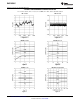
• Resolution 12 bits
outputs power up to zero volts and remain there until
• INL ±8 LSB (max)
there is a valid write to the device. The power-down
feature of the DAC128S085 allows each DAC to be
• DNL +0.75 / −0.4 LSB (max)
independently powered with three different
• Settling Time 8.5 μs (max)
termination options. With all the DAC channels
• Zero Code Error +15 mV (max)
powered down, power consumption reduces to less
than 0.3 µW at 3V and less than 1 µW at 5V. The low
• Full-Scale Error −0.75 %FSR (max)
power consumption and small packages of the
• Supply Power
DAC128S085 make it an excellent choice for use in
– 1.95 mW (3V) / 4.85 mW (5V) typ
battery operated equipment.
– Power Down 0.3 μW (3V) / 1 μW (5V) typ
1
Please be aware that an important notice concerning availability, standard warranty, and use in critical applications of
Texas Instruments semiconductor products and disclaimers thereto appears at the end of this data sheet.
2SPI is a trademark of Motorola, Inc..
3All other trademarks are the property of their respective owners.
PRODUCTION DATA information is current as of publication date.
Copyright © 2007–2013, Texas Instruments Incorporated
Products conform to specifications per the terms of the Texas
Instruments standard warranty. Production processing does not
necessarily include testing of all parameters.