
Datasheet


DAC7565
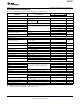
24-BitShiftRegister
SYNC
SCLK
D
IN
DataBufferA
DACRegisterA
DataBufferB
DACRegisterB
DataBufferC
DACRegisterC
DataBufferD
DACRegisterD
AV
DD
Buffer
Control
Register
Control
ControlLogic
2.5V
Reference
Power-Down
ControlLogic
12-BitDAC
12-BitDAC
12-BitDAC
12-BitDAC
V A
OUT
V B
OUT
V C
OUT
V D
OUT
GND
LDAC ENABLE
RSTSEL
RST
DAC7565
V
REF REF
H/V OUT
IOV
DD
V
REF
L
DAC7565
www.ti.com
SBAS412B –FEBRUARY 2008–REVISED MARCH 2011
12-Bit, Quad Channel, Ultra-Low Glitch, Voltage Output
Digital-to-Analog Converter with 2.5V, 2ppm/°C Internal Reference
Check for Samples: DAC7565
1
FEATURES
DESCRIPTION
The DAC7565 is a low-power, voltage-output,
234
• Relative Accuracy: 0.5LSB
four-channel, 12-bit digital-to-analog converter (DAC).
• Glitch Energy: 0.15nV-s
The device includes a 2.5V, 2ppm/°C internal
• Internal Reference:
reference (enabled by default), giving a full-scale
output voltage range of 2.5V. The internal reference
– 2.5V Reference Voltage (enabled by default)
has an initial accuracy of 0.02% and can source up to
– 0.004% Initial Accuracy (typ)
20mA at the V
REF
H/V
REF
OUT pin. The device is
– 2ppm/°C Temperature Drift (typ)
monotonic, provides very good linearity, and
minimizes undesired code-to-code transient voltages
– 5ppm/°C Temperature Drift (max)
(glitch). The DAC7565 uses a versatile 3-wire serial
– 20mA Sink/Source Capability
interface that operates at clock rates up to 50MHz.
• Power-On Reset to Zero-Scale or Mid-Scale
The interface is compatible with standard SPI™,
QSPI™, Microwire™, and digital signal processor
• Asynchronous Clear to Zero-Scale or
(DSP) interfaces.
Mid-Scale
• Ultra-Low Power Operation: 1mA at 5V
The DAC7565 incorporates a power-on-reset circuit
that ensures the DAC output powers up at either
• Wide Power-Supply Range: +2.7V to +5.5V
zero-scale or mid-scale until a valid code is written to
• 12-Bit Monotonic Over Temperature Range
the device. The device contains a power-down
• Settling Time: 10μs to ±0.024% Full-Scale
feature, accessed over the serial interface, that
Range (FSR)
reduces the current consumption of the device to
1.3μA at 5V. Power consumption is 2.9mW at 3V,
• Low-Power Serial Interface with
reducing to 1.5μW in power-down mode. The low
Schmitt-Triggered Inputs: Up to 50MHz
power consumption, internal reference, and small
• On-Chip Output Buffer Amplifier with
footprint make this device ideal for portable,
Rail-to-Rail Operation
battery-operated equipment.
• 1.8V to 5.5V Logic Compatibility
The DAC7565 is drop-in and functionally compatible
• Temperature Range: –40°C to +105°C
with the DAC8165 and DAC8565, and functionally
compatible with the DAC7564, DAC8164 and
APPLICATIONS
DAC8564. All these devices are available in a
TSSOP-16 package.
• Portable Instrumentation
• Closed-Loop Servo-Control
• Process Control, PLCs
• Data Acquisition Systems
• Programmable Attenuation
• PC Peripherals
RELATED
DEVICES 16-BIT 14-BIT 12-BIT
Pin and
Functionally DAC8565 DAC8165 DAC7565
Compatible
Functionally
DAC8564 DAC8164 DAC7564
Compatible
1
Please be aware that an important notice concerning availability, standard warranty, and use in critical applications of Texas
Instruments semiconductor products and disclaimers thereto appears at the end of this data sheet.
2SPI, QSPI are trademarks of Motorola, Inc.
3Microwire is a trademark of National Semiconductor.
4All other trademarks are the property of their respective owners.
PRODUCTION DATA information is current as of publication date.
Copyright © 2008–2011, Texas Instruments Incorporated
Products conform to specifications per the terms of the Texas
Instruments standard warranty. Production processing does not
necessarily include testing of all parameters.