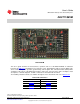
User's Guide SBAU165A – February 2010 – Revised May 2011 DAC7718EVM DAC7718EVM This user's guide describes the characteristics, operation, and use of the DAC7718EVM, an evaluation board for the DAC7718. The DAC7718 is a low-power, octal, 12-bit digital-to-analog converter (DAC). This device features low-power operation, good linearity, and low glitch. This evaluation module (EVM) allows evaluation of all aspects of the DAC7718 and gives control over every pin on the device.
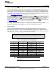
EVM Overview 1 2 3 4 5 6 7 www.ti.com Contents EVM Overview ............................................................................................................... Analog Interface ............................................................................................................. Digital Interface .............................................................................................................. Power Supplies ..................................................................
Analog Interface www.ti.com 2 Analog Interface For maximum flexibility, the DAC7718EVM can interface to multiple analog sources. Samtec part numbers SSW-110-22-F-D-VS-K and TSM-110-01-T-DV-P provides a 10-pin, dual-row, header at J1. This header provides access to the analog input and output pins of the DAC. An additional connector, J4, and test points are added to the evaluation module to allow access to all of the analog pins on the DAC. Consult Samtec at http://www.samtec.
Digital Interface 3 www.ti.com Digital Interface The DAC7718EVM is a serial input data converter. The evaluation module is designed for interfacing to multiple control platforms. 3.1 Serial Data Interface Samtec part numbers SSW-110-22-F-D-VS-K and TSM-110-01-T-DV-P provide a 10-pin, dual-row, header/socket combination at J2. This header/socket provides access to the digital control and serial data pins from both J2A (top side) and J2B (bottom side) of the connector.
Power Supplies www.ti.com The SCLK signal and the CS signal can each be controlled by multiple pins on J2. Pins J2.3 and J2.5 have been shorted together to control SCLK. J2.1, 2.7 and J2.9 have been shorted together to control CS. Pins J2.2, J2.6, J2.8, J2.12, J2.14, J2.15, J2.17, and J2.19 have weak pull-up/-down resistors. These resistors provide default settings for many of the control pins. These signals can be controlled through the digital interface or jumpers found directly on the EVM.
Voltage Reference www.ti.com The digital and analog ground inputs are short-circuited internally through a ground plane. The digital supply voltage (DVDD) for the DAC7718 is selectable between +5VD and +3.3VD via the JP11 jumper. Test point TP10 can be used to verify the digital supply voltage selected. Care must be taken to ensure that the EVM is not configured to be in a state where VREF is greater than DVDD. Diodes are put into place (D1 and D2) to add protection to the part.
EVM Operation www.ti.com 6 EVM Operation This section provides information on the analog input, digital control, and general operating conditions of the DAC7718EVM. 6.1 Analog Output The DAC7718 has eight analog outputs that are available through the J1 header. Each of these output are referenced to the board ground. The OFFSET-A and OFFSET-B analog outputs are routed to TP5 and TP6. The OFFSET feature can only be used in bipolar mode.
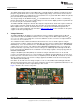
EVM Operation www.ti.com Figure 2 and Figure 3 show the default jumper conditions for bipolar and unipolar modes, respectively. Figure 2. DAC7718EVM Default Jumper Locations for Bipolar Mode Figure 3.
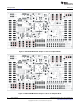
Schematics and Layout www.ti.com Jumpers JP1 and JP2 are used to control the reference voltage for group A. JP1 is selectable by connecting a jumper across pins 1 and 2 (2.5V) or 2 and 3 (5.0V). By default, a jumper is placed across pins 1 and 2 to enable the 2.5V reference. JP2 selects whether to use the onboard reference selected by JP1 (shunt pins 2 and 3) or use an external reference (shunt pins 1 and 2) from pin J1.18. Jumper JP3 and JP4 are used to control the reference voltage for group B.
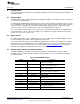
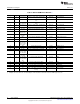
Schematics and Layout www.ti.com space Table 6. DAC7718EVM Bill of Materials (1) (1) (2) 10 Item No. Qty Ref Des Description Manufacturer 1 5 C1, C12, C13, C14, C15 Capacitor, ceramic, 10μF, 25V X5R 1206 10% Panasonic ECJ-3YB1E106K Mfr Part Number 2 2 C2, C22 Capacitor, ceramic, 0.1μF, 16V 0603 X7R 10% Panasonic ECJ-1VB1C104K 3 6 C3, C9, C10, C11, C18, C19 Capacitor, ceramic, 1.
Revision History www.ti.com Revision History Changes from Original (February, 2010) to A Revision ................................................................................................. Page • Updated Table 4 .......................................................................................................................... 5 NOTE: Page numbers for previous revisions may differ from page numbers in the current version.
1 8 7 DVDD Input Com NC DNC DNC NC Vin TEMP 0.1uF 3 Com D 3 C2 NC 4 2 2 Com 5 GND 1 Output 8 C1 10uF REF5V 6 Com JP1 REFASel2 REF2.5V C3 1uF REF5050 JP2 REF5V C4 10uF JP3 IOVDD AVDD 1 8 7 U2 Vin C18 3 1uF GND 2 DNC DNC NC 8V TEMP REF2.5V 6 Vout AVSS C12 C13 10uF 10uF REF2.5V REFBSel2 D R2 REF_B 2K C16 10uF REFBSel1 C14 10uF D2 DIODE-SCHOTTKY TP4 REF_B C15 10uF TP1 REF2.
Evaluation Board/Kit Important Notice Texas Instruments (TI) provides the enclosed product(s) under the following conditions: This evaluation board/kit is intended for use for ENGINEERING DEVELOPMENT, DEMONSTRATION, OR EVALUATION PURPOSES ONLY and is not considered by TI to be a finished end-product fit for general consumer use. Persons handling the product(s) must have electronics training and observe good engineering practice standards.
IMPORTANT NOTICE Texas Instruments Incorporated and its subsidiaries (TI) reserve the right to make corrections, modifications, enhancements, improvements, and other changes to its products and services at any time and to discontinue any product or service without notice. Customers should obtain the latest relevant information before placing orders and should verify that such information is current and complete.