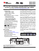
DAC8562, DAC8563 DAC8162, DAC8163 DAC7562, DAC7563 www.ti.com SLAS719D – AUGUST 2010 – REVISED AUGUST 2012 DUAL 16-/14-/12-BIT, ULTRALOW-GLITCH, LOW-POWER, BUFFERED, VOLTAGE-OUTPUT DAC WITH 2.5-V, 4-PPM/°C INTERNAL REFERENCE IN SMALL 3-MM × 3-MM SON Check for Samples: DAC8562, DAC8563, DAC8162, DAC8163, DAC7562, DAC7563 FEATURES DESCRIPTION • The DAC856x, DAC816x, and DAC756x are lowpower, voltage-output, dual-channel, 16-, 14-, and 12bit digital-to-analog converters (DACs), respectively.
DAC8562, DAC8563 DAC8162, DAC8163 DAC7562, DAC7563 SLAS719D – AUGUST 2010 – REVISED AUGUST 2012 www.ti.com This integrated circuit can be damaged by ESD. Texas Instruments recommends that all integrated circuits be handled with appropriate precautions. Failure to observe proper handling and installation procedures can cause damage. ESD damage can range from subtle performance degradation to complete device failure.
DAC8562, DAC8563 DAC8162, DAC8163 DAC7562, DAC7563 www.ti.com SLAS719D – AUGUST 2010 – REVISED AUGUST 2012 ABSOLUTE MAXIMUM RATINGS (1) Over operating free-air temperature range (unless otherwise noted). AVDD to GND VALUE UNIT –0.3 to 6 V CLR, DIN, LDAC, SCLK and SYNC input voltage to GND –0.3 to AVDD + 0.3 V VOUT to GND –0.3 to AVDD + 0.3 V VREFIN/VREFOUT to GND –0.3 to AVDD + 0.
DAC8562, DAC8563 DAC8162, DAC8163 DAC7562, DAC7563 SLAS719D – AUGUST 2010 – REVISED AUGUST 2012 www.ti.com ELECTRICAL CHARACTERISTICS At AVDD = 2.7 V to 5.5 V and TA = –40°C to 125°C (unless otherwise noted). PARAMETER STATIC PERFORMANCE TEST CONDITIONS MIN Resolution DAC856x Using line passing through codes 512 and 65,024 Differential nonlinearity 16-bit monotonic UNIT ±4 ±12 LSB ±0.2 ±1 LSB ±1 ±3 LSB ±0.1 ±0.5 LSB ±0.3 ±0.75 LSB ±0.05 ±0.
DAC8562, DAC8563 DAC8162, DAC8163 DAC7562, DAC7563 www.ti.com SLAS719D – AUGUST 2010 – REVISED AUGUST 2012 ELECTRICAL CHARACTERISTICS (continued) At AVDD = 2.7 V to 5.5 V and TA = –40°C to 125°C (unless otherwise noted). PARAMETER TEST CONDITIONS MIN TYP MAX UNIT REFERENCE External VREF = 2.
DAC8562, DAC8563 DAC8162, DAC8163 DAC7562, DAC7563 SLAS719D – AUGUST 2010 – REVISED AUGUST 2012 www.ti.com PIN CONFIGURATIONS DGS (Top View) DSC (Top View) VOUTA 1 10 VOUTB 2 VREFIN/VREFOUT VOUTA 1 10 9 AVDD VOUTB 2 9 AVDD GND 3 8 DIN LDAC 4 7 SCLK 6 SYNC GND 3 8 DIN LDAC 4 7 SCLK CLR 5 6 SYNC CLR 5 MSOP Package (1) Thermal Pad (1) VREFIN/VREFOUT SON Package It is recommended to connect the thermal pad to the ground plane for better thermal dissipation.
DAC8562, DAC8563 DAC8162, DAC8163 DAC7562, DAC7563 www.ti.com SLAS719D – AUGUST 2010 – REVISED AUGUST 2012 TIMING DIAGRAM t2 t1 SCLK t6 t4 t5 t3 t7 t8 SYNC t10 t9 DB23 DIN DB0 t12 t11 LDAC(1) LDAC(2) t13 CLR t14 VOUT (1) Asynchronous LDAC update mode. For more information, see the LDAC Functionality section. (2) Synchronous LDAC update mode; LDAC remains low. For more information, see the LDAC Functionality section. Figure 1. Serial Write Operation TIMING REQUIREMENTS (1) (2) At AVDD = 2.
DAC8562, DAC8563 DAC8162, DAC8163 DAC7562, DAC7563 SLAS719D – AUGUST 2010 – REVISED AUGUST 2012 www.ti.com TABLES OF GRAPHS Table 3. Typical Characteristics: Internal Reference Performance POWER-SUPPLY VOLTAGE MEASUREMENT FIGURE NUMBER Internal Reference Voltage vs Temperature Figure 2 Internal Reference Voltage Temperature Drift Histogram Figure 3 Internal Reference Voltage vs Load Current 5.
DAC8562, DAC8563 DAC8162, DAC8163 DAC7562, DAC7563 www.ti.com SLAS719D – AUGUST 2010 – REVISED AUGUST 2012 Table 4. Typical Characteristics: DAC Static Performance (continued) MEASUREMENT POWER-SUPPLY VOLTAGE FIGURE NUMBER POWER-DOWN CURRENT Power-Down Current vs Temperature Power-Down Current vs Power-Supply Voltage Power-Down Current vs Temperature 5.5 V Figure 28 2.7 V – 5.5 V Figure 29 2.
DAC8562, DAC8563 DAC8162, DAC8163 DAC7562, DAC7563 SLAS719D – AUGUST 2010 – REVISED AUGUST 2012 www.ti.com Table 5. Typical Characteristics: DAC Dynamic Performance MEASUREMENT POWER-SUPPLY VOLTAGE FIGURE NUMBER CHANNEL-TO-CHANNEL CROSSTALK Channel-to-Channel Crosstalk 5-V Rising Edge 5-V Falling Edge 5.5 V Figure 43 Figure 44 CLOCK FEEDTHROUGH Clock Feedthrough 500 kHz, Midscale 5.5 V Figure 48 2.
DAC8562, DAC8563 DAC8162, DAC8163 DAC7562, DAC7563 www.ti.com SLAS719D – AUGUST 2010 – REVISED AUGUST 2012 TYPICAL CHARACTERISTICS: Internal Reference At TA = 25°C, AVDD = 5.5 V, gain = 2 and VREFOUT, unloaded unless otherwise noted. INTERNAL REFERENCE VOLTAGE vs TEMPERATURE INTERNAL REFERENCE VOLTAGE TEMPERATURE DRIFT HISTOGRAM 30 2.505 2.504 25 2.503 Population (%) 2.501 2.500 2.499 2.498 2.497 10 5 0 2.
DAC8562, DAC8563 DAC8162, DAC8163 DAC7562, DAC7563 SLAS719D – AUGUST 2010 – REVISED AUGUST 2012 www.ti.com TYPICAL CHARACTERISTICS: DAC at AVDD = 5.5 V At TA = 25°C, 5-V external reference used, gain = 1 and DAC output not loaded, unless otherwise noted. LINEARITY ERROR vs DIGITAL INPUT CODE (–40°C) DIFFERENTIAL LINEARITY ERROR vs DIGITAL INPUT CODE (–40°C) 12 1.0 9 0.8 0.6 DNL Error (LSB) INL Error (LSB) 6 3 0 −3 0.4 0.2 0.0 −0.2 −0.4 −6 −0.
DAC8562, DAC8563 DAC8162, DAC8163 DAC7562, DAC7563 www.ti.com SLAS719D – AUGUST 2010 – REVISED AUGUST 2012 TYPICAL CHARACTERISTICS: DAC at AVDD = 5.5 V (continued) At TA = 25°C, 5-V external reference used, gain = 1 and DAC output not loaded, unless otherwise noted. LINEARITY ERROR vs TEMPERATURE DIFFERENTIAL LINEARITY ERROR vs TEMPERATURE 12 1.0 INL Max INL Min 9 DNL Max DNL Min 0.8 0.6 DNL Error (LSB) INL Error (LSB) 6 3 0 −3 0.4 0.2 0.0 −0.2 −0.4 −6 −0.
DAC8562, DAC8563 DAC8162, DAC8163 DAC7562, DAC7563 SLAS719D – AUGUST 2010 – REVISED AUGUST 2012 www.ti.com TYPICAL CHARACTERISTICS: DAC at AVDD = 5.5 V (continued) At TA = 25°C, 5-V external reference used, gain = 1 and DAC output not loaded, unless otherwise noted. 0.45 1.2 Power−Supply Current (mA) 1.3 0.40 0.35 0.30 0.25 0.20 0.15 0.10 0.9 0.8 0.7 5 20 35 50 65 Temperature (°C) 80 95 Internal reference enabled DACs at midscale code, Gain = 2 0.
DAC8562, DAC8563 DAC8162, DAC8163 DAC7562, DAC7563 www.ti.com SLAS719D – AUGUST 2010 – REVISED AUGUST 2012 TYPICAL CHARACTERISTICS: DAC at AVDD = 5.5 V (continued) At TA = 25°C, 5-V external reference used, gain = 1 and DAC output not loaded, unless otherwise noted. POWER-SUPPLY CURRENT vs POWER-SUPPLY VOLTAGE POWER-SUPPLY CURRENT vs POWER-SUPPLY VOLTAGE 0.50 1.2 Power−Supply Current (mA) Power−Supply Current (mA) 0.45 1.3 VREFIN = 2.5 V DACs at midscale code, Gain = 1 0.40 0.35 0.30 0.25 0.20 0.
DAC8562, DAC8563 DAC8162, DAC8163 DAC7562, DAC7563 SLAS719D – AUGUST 2010 – REVISED AUGUST 2012 www.ti.com TYPICAL CHARACTERISTICS: DAC at AVDD = 5.5 V (continued) At TA = 25°C, 5-V external reference used, gain = 1 and DAC output not loaded, unless otherwise noted. FULL-SCALE SETTLING TIME: RISING EDGE FULL-SCALE SETTLING TIME: FALLING EDGE LDAC Trigger (5 V/div) LDAC Trigger (5 V/div) Large Signal VOUT (2 V/div) Large Signal VOUT (2 V/div) Small Signal Settling (1.22 mV/div = 0.
DAC8562, DAC8563 DAC8162, DAC8163 DAC7562, DAC7563 www.ti.com SLAS719D – AUGUST 2010 – REVISED AUGUST 2012 TYPICAL CHARACTERISTICS: DAC at AVDD = 5.5 V (continued) At TA = 25°C, 5-V external reference used, gain = 1 and DAC output not loaded, unless otherwise noted. GLITCH ENERGY RISING EDGE, 1-LSB STEP GLITCH ENERGY FALLING EDGE, 1-LSB STEP LDAC Trigger (5 V/div) LDAC Trigger (5 V/div) LDAC Feedthrough Glitch Impulse » 0.
DAC8562, DAC8563 DAC8162, DAC8163 DAC7562, DAC7563 SLAS719D – AUGUST 2010 – REVISED AUGUST 2012 www.ti.com TYPICAL CHARACTERISTICS: DAC at AVDD = 5.5 V (continued) At TA = 25°C, 5-V external reference used, gain = 1 and DAC output not loaded, unless otherwise noted. CHANNEL-TO-CHANNEL CROSSTALK 5-V RISING EDGE CHANNEL-TO-CHANNEL CROSSTALK 5-V FALLING EDGE LDAC Trigger (5 V/div) LDAC Trigger (5 V/div) VOUTB (1 V/div) 6.
DAC8562, DAC8563 DAC8162, DAC8163 DAC7562, DAC7563 www.ti.com SLAS719D – AUGUST 2010 – REVISED AUGUST 2012 TYPICAL CHARACTERISTICS: DAC at AVDD = 3.6 V At TA = 25°C, 3.3-V external reference used, gain = 1 and DAC output not loaded, unless otherwise noted. 0.50 1.3 0.45 1.2 0.40 0.35 0.30 0.25 0.20 0.15 0.10 1.0 0.9 0.8 0.7 5 20 35 50 65 Temperature (°C) 80 95 0.5 −40 −25 −10 110 125 5 20 35 50 65 Temperature (°C) 80 Figure 49. Figure 50.
DAC8562, DAC8563 DAC8162, DAC8163 DAC7562, DAC7563 SLAS719D – AUGUST 2010 – REVISED AUGUST 2012 www.ti.com TYPICAL CHARACTERISTICS: DAC at AVDD = 2.7 V At TA = 25°C, 2.5-V external reference used, gain = 1 and DAC output not loaded, unless otherwise noted. LINEARITY ERROR vs DIGITAL INPUT CODE (–40°C) DIFFERENTIAL LINEARITY ERROR vs DIGITAL INPUT CODE (–40°C) 12 1.0 9 0.8 0.6 DNL Error (LSB) INL Error (LSB) 6 3 0 −3 0.4 0.2 0.0 −0.2 −0.4 −6 −0.
DAC8562, DAC8563 DAC8162, DAC8163 DAC7562, DAC7563 www.ti.com SLAS719D – AUGUST 2010 – REVISED AUGUST 2012 TYPICAL CHARACTERISTICS: DAC at AVDD = 2.7 V (continued) At TA = 25°C, 2.5-V external reference used, gain = 1 and DAC output not loaded, unless otherwise noted. LINEARITY ERROR vs TEMPERATURE DIFFERENTIAL LINEARITY ERROR vs TEMPERATURE 12 1.0 INL Max INL Min 9 DNL Max DNL Min 0.8 0.6 DNL Error (LSB) INL Error (LSB) 6 3 0 −3 0.4 0.2 0.0 −0.2 −0.4 −6 −0.
DAC8562, DAC8563 DAC8162, DAC8163 DAC7562, DAC7563 SLAS719D – AUGUST 2010 – REVISED AUGUST 2012 www.ti.com TYPICAL CHARACTERISTICS: DAC at AVDD = 2.7 V (continued) At TA = 25°C, 2.5-V external reference used, gain = 1 and DAC output not loaded, unless otherwise noted. POWER-SUPPLY CURRENT vs TEMPERATURE 0.40 1.3 0.35 1.2 Power−Supply Current (mA) Power−Supply Current (mA) POWER-SUPPLY CURRENT vs TEMPERATURE 0.30 0.25 0.20 0.15 0.10 0.05 1.1 1.0 0.9 0.8 0.7 0.
DAC8562, DAC8563 DAC8162, DAC8163 DAC7562, DAC7563 www.ti.com SLAS719D – AUGUST 2010 – REVISED AUGUST 2012 TYPICAL CHARACTERISTICS: DAC at AVDD = 2.7 V (continued) At TA = 25°C, 2.5-V external reference used, gain = 1 and DAC output not loaded, unless otherwise noted. POWER-DOWN CURRENT vs TEMPERATURE DAC OUTPUT VOLTAGE vs LOAD CURRENT 3.0 4 Full scale Mid scale Zero scale 3 2.0 Output Voltage (V) Power−Down Current (µA) Typical channel shown 2.5 1.5 1.0 0.5 2 1 0 0.
DAC8562, DAC8563 DAC8162, DAC8163 DAC7562, DAC7563 SLAS719D – AUGUST 2010 – REVISED AUGUST 2012 www.ti.com TYPICAL CHARACTERISTICS: DAC at AVDD = 2.7 V (continued) At TA = 25°C, 2.5-V external reference used, gain = 1 and DAC output not loaded, unless otherwise noted. GLITCH ENERGY RISING EDGE, 1-LSB STEP GLITCH ENERGY FALLING EDGE, 1-LSB STEP LDAC Trigger (5 V/div) LDAC Trigger (5 V/div) LDAC Feedthrough Glitch Impulse » 0.
DAC8562, DAC8563 DAC8162, DAC8163 DAC7562, DAC7563 www.ti.com SLAS719D – AUGUST 2010 – REVISED AUGUST 2012 TYPICAL CHARACTERISTICS: DAC at AVDD = 2.7 V (continued) At TA = 25°C, 2.5-V external reference used, gain = 1 and DAC output not loaded, unless otherwise noted.
DAC8562, DAC8563 DAC8162, DAC8163 DAC7562, DAC7563 SLAS719D – AUGUST 2010 – REVISED AUGUST 2012 www.ti.com THEORY OF OPERATION DIGITAL-TO-ANALOG CONVERTER (DAC) The DAC756x, DAC816x, and DAC856x architecture consists of two string DACs, each followed by an output buffer amplifier. The devices include an internal 2.5-V reference with 4-ppm/°C temperature drift performance. Figure 88 shows a principal block diagram of the DAC architecture.
DAC8562, DAC8563 DAC8162, DAC8163 DAC7562, DAC7563 www.ti.com SLAS719D – AUGUST 2010 – REVISED AUGUST 2012 Resistor String The resistor string section is shown in Figure 89. It is simply a string of resistors, each of value R. The code loaded into the DAC register determines at which node on the string the voltage is tapped off to be fed into the output amplifier by closing one of the switches connecting the string to the amplifier. The resistor string architecture guarantees monotonicity.
DAC8562, DAC8563 DAC8162, DAC8163 DAC7562, DAC7563 SLAS719D – AUGUST 2010 – REVISED AUGUST 2012 www.ti.com INTERNAL REFERENCE The DAC756x, DAC816x, and DAC856x include a 2.5-V internal reference that is disabled by default. The internal reference is externally available at the VREFIN/VREFOUT pin. The internal reference output voltage is 2.5 V and can sink and source up to 20 mA. A minimum 150-nF capacitor is recommended between the reference output and GND for noise filtering.
DAC8562, DAC8563 DAC8162, DAC8163 DAC7562, DAC7563 www.ti.com SLAS719D – AUGUST 2010 – REVISED AUGUST 2012 POWER-ON RESET Power-On Reset to Zero-scale The DAC7562, DAC8162, and DAC8562 contain a power-on-reset circuit that controls the output voltage during power up. All device registers are reset as shown in Table 6. At power up all DAC registers are filled with zeros and the output voltages of all DAC channels are set to zero volts.
DAC8562, DAC8563 DAC8162, DAC8163 DAC7562, DAC7563 SLAS719D – AUGUST 2010 – REVISED AUGUST 2012 www.ti.com Power-On Reset (POR) Levels When the device powers up, a POR circuit sets the device in default mode as shown in Table 6. The POR circuit requires specific AVDD levels, as indicated in Figure 91, to ensure discharging of internal capacitors and to reset the device on power up. In order to ensure a power-on reset, AVDD must be below 0.7 V for at least 1 ms. When AVDD drops below 2.
DAC8562, DAC8563 DAC8162, DAC8163 DAC7562, DAC7563 www.ti.com SLAS719D – AUGUST 2010 – REVISED AUGUST 2012 SERIAL INTERFACE The DAC756x, DAC816x, and DAC856x have a 3-wire serial interface (SYNC, SCLK, and DIN; see the Pin Descriptions) compatible with SPI, QSPI, and Microwire interface standards, as well as most DSPs. See the Serial Write Operation timing diagram (Figure 1) for an example of a typical write sequence.
DAC8562, DAC8563 DAC8162, DAC8163 DAC7562, DAC7563 SLAS719D – AUGUST 2010 – REVISED AUGUST 2012 www.ti.com Input Shift Register The input shift register (SR) of the DAC856x, DAC816x, and DAC756x is 24 bits wide (as shown in Table 8, Table 9, and Table 10, respectively), and consists of two don’t care bits (DB23 to DB22), three command bits (DB21 to DB19), three address bits (DB18 to DB16), and 16 data bits (DB15 to DB0). The 16 data bits comprise the 16-, 14-, or 12-bit input code. Table 8.
DAC8562, DAC8563 DAC8162, DAC8163 DAC7562, DAC7563 www.ti.com SLAS719D – AUGUST 2010 – REVISED AUGUST 2012 Table 13.
DAC8562, DAC8563 DAC8162, DAC8163 DAC7562, DAC7563 SLAS719D – AUGUST 2010 – REVISED AUGUST 2012 www.ti.com GAIN REGISTERS The gain register controls the GAIN setting in the DAC transfer function: æD ö VO UT = ç IN ´ VREF ´ Gain n ÷ è 2 ø (2) The DAC756x, DAC816x, and DAC856x have a gain register for each channel. The gain for each channel, in Equation 2, is either 1 or 2.
DAC8562, DAC8563 DAC8162, DAC8163 DAC7562, DAC7563 www.ti.com SLAS719D – AUGUST 2010 – REVISED AUGUST 2012 POWER-DOWN MODES The DAC756x, DAC816x, and DAC856x have two separate sets of power-down commands. One set is for the DAC channels and the other set is for the internal reference. The internal reference is forced to a powered down state while both DAC channels are powered down, and is only enabled if any DAC channel is also in normal mode of operation.
DAC8562, DAC8563 DAC8162, DAC8163 DAC7562, DAC7563 SLAS719D – AUGUST 2010 – REVISED AUGUST 2012 www.ti.com SOFTWARE RESET FUNCTION The DAC756x, DAC816x, and DAC856x contain a software reset feature. The software reset function uses command 101. The software reset command contains two reset modes which are software-programmable by setting bit DB0 in the shift register. Table 13 and/or Table 19 and Table 20 show the available software reset commands. Table 19.
DAC8562, DAC8563 DAC8162, DAC8163 DAC7562, DAC7563 www.ti.com SLAS719D – AUGUST 2010 – REVISED AUGUST 2012 Alternatively, all DAC outputs can be updated simultaneously using the built-in software function of LDAC. The LDAC register offers additional flexibility and control by allowing the selection of which DAC channel(s) should be updated simultaneously when the LDAC pin is being brought low.
DAC8562, DAC8563 DAC8162, DAC8163 DAC7562, DAC7563 SLAS719D – AUGUST 2010 – REVISED AUGUST 2012 www.ti.com APPLICATION INFORMATION INTERNAL REFERENCE The internal reference of the DAC756x, DAC816x, and DAC856x does not require an external load capacitor for stability because it is stable without any capacitive load. However, for improved noise performance, an external load capacitor of 150 nF or larger connected to the VREFIN/VREFOUT output is recommended.
DAC8562, DAC8563 DAC8162, DAC8163 DAC7562, DAC7563 www.ti.com SLAS719D – AUGUST 2010 – REVISED AUGUST 2012 Load Regulation Load regulation is defined as the change in reference output voltage as a result of changes in load current. The load regulation of the internal reference is measured using force and sense contacts as shown in Figure 95.
DAC8562, DAC8563 DAC8162, DAC8163 DAC7562, DAC7563 SLAS719D – AUGUST 2010 – REVISED AUGUST 2012 www.ti.com UP TO ±15-V BIPOLAR OUTPUT USING THE DAC8562 The DAC8562 is designed to be operate from a single power supply providing a maximum output range of AVDD volts. However, the DAC can be placed in the configuration shown in Figure 96 in order to be designed into bipolar systems. Depending on the ratio of the resistor values, the output of the circuit can range anywhere from ±5 V to ±15 V.
DAC8562, DAC8563 DAC8162, DAC8163 DAC7562, DAC7563 www.ti.com SLAS719D – AUGUST 2010 – REVISED AUGUST 2012 PLC ANALOG OUTPUT MODULE USING THE DAC8562 The DAC8562 can be mated with one of TI's 0- to 20-mA voltage-to-current transmitters to create a low-cost, programmable current source for use in PLC applications. One specific example includes combining the DAC8562 with the XTR111 to create a voltage-to-current solution.
DAC8562, DAC8563 DAC8162, DAC8163 DAC7562, DAC7563 SLAS719D – AUGUST 2010 – REVISED AUGUST 2012 www.ti.com MICROPROCESSOR INTERFACING DAC756x/DAC816x/DAC856x to an MSP430 USI Interface Figure 98 shows a serial interface between the DAC756x, DAC816x, or DAC856x and a typical MSP430 USI port such as the one found on the MSP430F2013. The port is configured in SPI master mode by setting bits 3, 5, 6, and 7 in USICTL0.
DAC8562, DAC8563 DAC8162, DAC8163 DAC7562, DAC7563 www.ti.com SLAS719D – AUGUST 2010 – REVISED AUGUST 2012 LAYOUT A precision analog component requires careful layout, adequate bypassing, and clean, well-regulated power supplies. The DAC756x, DAC816x, and DAC856x offer single-supply operation, and are often used in close proximity with digital logic, microcontrollers, microprocessors, and digital signal processors.
DAC8562, DAC8563 DAC8162, DAC8163 DAC7562, DAC7563 SLAS719D – AUGUST 2010 – REVISED AUGUST 2012 www.ti.com PARAMETER DEFINITIONS With the increased complexity of many different specifications listed in product data sheets, this section summarizes selected specifications related to digital-to-analog converters. STATIC PERFORMANCE Static performance parameters are specifications such as differential nonlinearity (DNL) or integral nonlinearity (INL).
DAC8562, DAC8563 DAC8162, DAC8163 DAC7562, DAC7563 www.ti.com SLAS719D – AUGUST 2010 – REVISED AUGUST 2012 Relative Accuracy or Integral Nonlinearity (INL) Relative accuracy or integral nonlinearity (INL) is defined as the maximum deviation between the real transfer function and a straight line passing through the endpoints of the ideal DAC transfer function. INL is measured in LSBs. Resolution Generally, the DAC resolution can be expressed in different forms.
DAC8562, DAC8563 DAC8162, DAC8163 DAC7562, DAC7563 SLAS719D – AUGUST 2010 – REVISED AUGUST 2012 www.ti.com DYNAMIC PERFORMANCE Dynamic performance parameters are specifications such as settling time or slew rate, which are important in applications where the signal rapidly changes and/or high frequency signals are present.
DAC8562, DAC8563 DAC8162, DAC8163 DAC7562, DAC7563 www.ti.com SLAS719D – AUGUST 2010 – REVISED AUGUST 2012 REVISION HISTORY Changes from Revision C (June 2011, first official release) to Revision D Page • Replaced text "QFN" with "SON" (name change only, package/orderable did not change) ................................................ 1 • Typical power-down current consumption changed from 10 nA to 550 nA. .........................................................................
PACKAGE OPTION ADDENDUM www.ti.
PACKAGE OPTION ADDENDUM www.ti.
PACKAGE OPTION ADDENDUM www.ti.com 10-Oct-2013 Important Information and Disclaimer:The information provided on this page represents TI's knowledge and belief as of the date that it is provided. TI bases its knowledge and belief on information provided by third parties, and makes no representation or warranty as to the accuracy of such information. Efforts are underway to better integrate information from third parties.
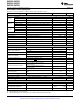
PACKAGE MATERIALS INFORMATION www.ti.com 24-Apr-2013 TAPE AND REEL INFORMATION *All dimensions are nominal Device Package Package Pins Type Drawing DAC7562SDGSR VSSOP DGS 10 SPQ Reel Reel A0 Diameter Width (mm) (mm) W1 (mm) B0 (mm) K0 (mm) P1 (mm) W Pin1 (mm) Quadrant 2500 330.0 12.4 5.3 3.3 1.3 8.0 12.0 Q1 DAC7562SDGST VSSOP DGS 10 250 180.0 12.4 5.3 3.3 1.3 8.0 12.0 Q1 DAC7562SDSCR WSON DSC 10 3000 330.0 12.4 3.3 3.3 1.1 8.0 12.
PACKAGE MATERIALS INFORMATION www.ti.com 24-Apr-2013 Device Package Package Pins Type Drawing SPQ Reel Reel A0 Diameter Width (mm) (mm) W1 (mm) B0 (mm) K0 (mm) P1 (mm) W Pin1 (mm) Quadrant DAC8562SDSCR WSON DSC 10 3000 330.0 12.4 3.3 3.3 1.1 8.0 12.0 Q2 DAC8562SDSCT WSON DSC 10 250 180.0 12.4 3.3 3.3 1.1 8.0 12.0 Q2 DAC8563SDGSR VSSOP DGS 10 2500 330.0 12.4 5.3 3.3 1.3 8.0 12.0 Q1 DAC8563SDGST VSSOP DGS 10 250 180.0 12.4 5.3 3.3 1.3 8.0 12.
PACKAGE MATERIALS INFORMATION www.ti.com 24-Apr-2013 Device Package Type Package Drawing Pins SPQ Length (mm) Width (mm) Height (mm) DAC8162SDSCT WSON DSC 10 250 210.0 185.0 35.0 DAC8163SDGSR VSSOP DGS 10 2500 370.0 355.0 55.0 DAC8163SDGST VSSOP DGS 10 250 220.0 205.0 50.0 DAC8163SDSCR WSON DSC 10 3000 367.0 367.0 35.0 DAC8163SDSCT WSON DSC 10 250 210.0 185.0 35.0 DAC8562SDGSR VSSOP DGS 10 2500 370.0 355.0 55.0 DAC8562SDGST VSSOP DGS 10 250 220.
IMPORTANT NOTICE Texas Instruments Incorporated and its subsidiaries (TI) reserve the right to make corrections, enhancements, improvements and other changes to its semiconductor products and services per JESD46, latest issue, and to discontinue any product or service per JESD48, latest issue. Buyers should obtain the latest relevant information before placing orders and should verify that such information is current and complete.