
Datasheet

www.ti.com
1 3
1 3
1 3
1 3
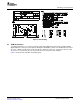
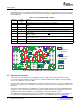
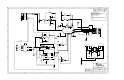
3.6 Schematic
EVM Operation
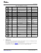
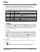
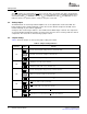
Table 4. Jumper Setting Function (continued)
Jumper
Reference Function
Setting
GPIO2/TOUT signal from J2-15 is routed to drive the LDAC signal of the DAC8871.
W6
GPIO1/ INT signal from J2-17 is routed to drive the LDAC signal of the DAC8871.
Allows the onboard REF102 output of +10 V to propagate through for the DAC8871’s voltage
reference high and low source (V
REF
H, V
REF
L).
W7
Disconnects the onboard REF102 output of +10 V used for the DAC8871’s voltage reference high
and low source (V
REF
H, V
REF
L).
Connect this jumper if trimming function is desired for U3. Trim potentiometer, R3, is not populated
by default; so, this jumper is not used.
W8
This is the default position. Trim potentiometer, R3, is not populated by default; so, this jumper is
not used.
Routes +3.3 VD for V
DD
to power digital voltage pin of DAC8871.
W9
Routes +5 VD for V
DD
to power the digital voltage pin of DAC8871.
Legend: Indicates the corresponding pins that are shorted or closed.
The DAC8871EVM evaluation module schematic appears on the following page.
SLAU233 – September 2007 DAC8871 Evaluation Module 13
Submit Documentation Feedback