
Datasheet

www.ti.com
DACModule
VCC
VSS
VCC
GND
GND
VDD
(J3)
(P3)
VDD
(J2)
(P2)
SCLK
W1
VSS
AGND
SDI
(J1)
(P1)
CS
VSS
±5VA
+3.3VD
FS
V
OUT
V
REF
L
V
DD
REF102
INA105
U2
U5A
+V
REF
-V
REF
TP1
VCC
TP2
V
REF
H
V
SS
V
CC
W3
DGND
LDAC
RST
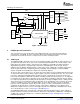
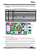
2 PCB Design and Performance
2.1 PCB Layout
PCB Design and Performance
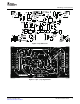
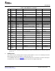
Figure 1. Block Diagram
This section discusses the layout design of the PCB and describes the physical and mechanical
characteristics of the EVM, as well as a brief description of the EVM test performance procedure
performed. Also included is the list of components used on this evaluation module.
The DAC8871EVM is designed to preserve the performance quality of the DAC, the device under test, as
specified in the data sheet. The key to a successful design implementation is the careful analysis of the
EVM’s physical restrictions and the elements that can contribute to the EVM’s potential performance
degradation. By properly selecting the right components and building the circuit correctly, obvious
attributes that can diminish EVM performance can be taken cared of during the schematic design phase.
Good circuit design includes adequate bypassing, identifying, and managing the analog and digital
signals, along with understanding the components mechanical attributes.
An obscure part of the design process can be the layout. The main concern is primarily with the placement
of components and the proper routing of signals. Bypass capacitors should be placed as close as possible
to the pins, and analog and digital signals should be properly separated from each other. Because the
power and ground plane is important, it should be carefully considered in the layout process. A solid plane
is ideal but if this is impractical, a split plane can be used. When considering a split plane design, analyze
the component placement and carefully split the board into its analog and digital sections, starting from the
device under test. The ground plane plays an important role in controlling the noise and other effects that
otherwise contributes to the error of the DAC output. To ensure that the return currents are handled
properly, route the appropriate signals only in their respective sections, meaning that the analog traces
should only lay directly above or below the analog section and the digital traces in the digital section.
Minimize the length of the traces, but use the biggest possible trace width that is allowable in the design.
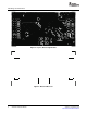
These design practices can be seen in Figure 2 through Figure 6 .
The DAC8871 EVM board is constructed on a two-layer printed-circuit board using a copper-clad FR-4
laminate material. The printed-circuit board has a dimension of 43,1800 mm (1.7000 inch) × 82,5500 mm
(3.2500 inch), and the board thickness is 1,5748 mm (0.062 inch). Figure 2 through Figure 6 show the
individual artwork layers.
4 DAC8871 Evaluation Module SLAU233 – September 2007
Submit Documentation Feedback