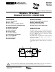
DCR DCR01 Series 01 DCR 01 SBVS013C – OCTOBER 2001 – REVISED MAY 2003 Miniature, 1W Isolated REGULATED DC/DC CONVERTERS FEATURES APPLICATIONS ● UL1950 RECOGNIZED ● ● ● ● ● DIP-18, SO-28 ● 53W/in3 (3.
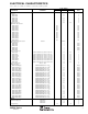
ELECTROSTATIC DISCHARGE SENSITIVITY ABSOLUTE MAXIMUM RATINGS Input Voltage: DCR0105 ............................................................................................ 7V DCR0112 .......................................................................................... 15V DCR0124 .......................................................................................... 29V Storage Temperature ......................................................
ELECTRICAL CHARACTERISTICS At TA = +25°C, VS = nominal, IO = 10mA, CO = 0.1µF, unless otherwise specified.
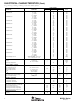
ELECTRICAL CHARACTERISTICS (Cont.) At TA = +25°C, VS = nominal, IO = 10mA, CO = 0.1µF, unless otherwise specified.
PIN CONFIGURATIONS Top View SO DIP VS 1 18 SYNC VS 1 28 SYNC NC 2 17 0VIN VS 2 27 0VIN NC 3 26 0VIN DCR01 DCR01U VREC 7 12 ERROR VREC 12 17 ERROR 0VOUT 8 11 ENABLE 0VOUT 13 16 ENABLE VO 9 10 DNC PIN DEFINITION (DIP) PIN DEFINITION (SO) PIN # PIN NAME PIN # PIN NAME 1 VS Voltage Input 1 VS 2 NC No Connection 2 VS Voltage Input 7 VREC Rectified Output 3 NC No Connection 8 0VOUT Output Ground 12 VREC Rectified Output 9 VO Voltage Output 13 VOUT
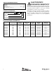
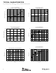
TYPICAL CHARACTERISTICS At TA = +25°C, VS = 5V, IO = 10mA, CFILTER = 1µF, CO = 0.1µF, unless otherwise specified. DCR0105 OUTPUT NOISE (100MHz Bandwidth) 18 80 16 70 14 60 12 Noise (mVp-p) Ripple Voltage (mVp-p) OUTPUT VOLTAGE RIPPLE (all “U”, all 5V Output “P” Devices, and DCR010503P) 10 8 6 40 30 20 4 10 2 0 0 0 20 40 60 80 0 100 20 40 60 80 Load (%) Load (%) DCR011203P AND DCR012403P OUTPUT VOLTAGE RIPPLE 3V OUTPUT EFFICIENCY (5V and 12V Input Devices) 30.0 70 25.
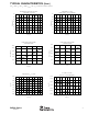
TYPICAL CHARACTERISTICS (Cont.) At TA = +25°C, VS = 5V, IO = 10mA, CFILTER = 1µF, CO = 0.1µF, unless otherwise specified. EFFICIENCY vs LOAD DCR0112405 “P” and “U” DEVICES 70 70 60 60 50 50 Efficiency (%) Efficiency (%) EFFICIENCY FOR 5V AND 12V INPUT “U” DEVICES, 5V OUTPUT 40 30 30 20 20 10 10 0 0 0 10 20 30 40 50 60 70 80 90 100 0 10 20 30 40 50 60 70 80 Load (%) Load (%) DCR011203P OUTPUT NOISE (100MHz Bandwidth) DCR011205P OUTPUT NOISE (100MHz Bandwidth) 120.
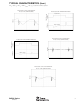
TYPICAL CHARACTERISTICS (Cont.) At TA = +25°C, VS = 5V, IO = 10mA, CFILTER = 1µF, CO = 0.1µF, unless otherwise specified. DCR0105 SERIES INPUT CURRENT REFLECTED NOISE (100MHz Bandwidth) LOAD vs VOUT (for all 5V Output Devices) 5.04 5.02 40mA/div VOUT (V) 5.00 4.98 4.96 4.94 4.
TYPICAL CHARACTERISTICS (Cont.) At TA = +25°C, VS = 5V, IO = 10mA, CFILTER = 1µF, CO = 0.1µF, unless otherwise specified.
FUNCTIONAL DESCRIPTION If devices are synchronized, it should be noted that all devices will draw maximum current simultaneously at start up. This can cause the input voltage to dip. Should it fall below the minimum input voltage, the devices may not start up. A 2.2µF capacitor (low ESR) should be connected as close to the device input pins as possible for the 5V input devices, and a 0.47µF capacitor for the 12V and 24V devices.
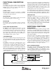
APPLICATION NOTES ERROR FLAG The DCR01 has an ERROR pin which provides a “power good” flag, as long as the internal regulator is in regulation. DCR01 SINGLE VOLTAGE OUTPUT The DCR01 can be used to provide a single voltage output by connecting, see Figure 1. The ERROR output signal will be pulled up to the value of VOUT for the particular DCR01 being used.
If the SYNC pin is being used, the tracking between device SYNC pins should be short to avoid stray capacitance. If the SYNC pin is not being used it is advisable to place a guard ring (connected to input ground) around this pin to avoid any noise pick up. The output should be taken from the device using ground and power planes. This will ensure minimum losses. A good quality low ESR capacitor placed as close as practicable across the input will reduce reflected ripple and ensure a smooth start up.
PACKAGE OPTION ADDENDUM www.ti.
PACKAGE OPTION ADDENDUM www.ti.com 28-Aug-2010 PREVIEW: Device has been announced but is not in production. Samples may or may not be available. OBSOLETE: TI has discontinued the production of the device. (2) Eco Plan - The planned eco-friendly classification: Pb-Free (RoHS), Pb-Free (RoHS Exempt), or Green (RoHS & no Sb/Br) - please check http://www.ti.com/productcontent for the latest availability information and additional product content details.
MECHANICAL DATA MPDI055 – APRIL 2001 NVE (R-PDIP-T10/18) PLASTIC DUAL-IN-LINE 0.920 (23,37) 0.880 (22,35) D 18 10 0.280 (7,11) 0.240 (6,10) D 1 9 Index Area E 0.070 (1,78) 0.045 (1,14) 0.195 (4,95) 0.115 (2,92) Base Plane –C– Seating Plane 0.325 (8,26) 0.300 (7,62) 0.210 (5,33) MAX E 0.005 (0,13) MIN 4 PL Full Lead D 0.100 (2,54) 0.022 (0,56) 0.014 (0,36) 0.010 (0,25) M C 0.150 (3,81) 0.115 (2,92) 0.300 (7,63) 0.014 (0,36) 0.008 (0,20) 0.015 (0,38) MIN 0.060 (1,52) 0.000 (0,00) 0.
MECHANICAL DATA MPDS106A – AUGUST 2001 – REVISED NOVEMBER 2001 DVB(R-PDSO-G12/28) –A– 28 PLASTIC SMALL-OUTLINE 18,10 17,70 11,20 10,82 C 0°–8° 15 1,27 0,40 F 7,60 7,40 –B– D 10,65 10,01 0,25 M B M Index Area 1 14 0,30 0,10 2,65 2,35 0,75 0,25 x 45° Base Plane –C– Seating Plane 1,27 G 0,32 0,23 0,51 0,33 0,10 0,25 M C A M B S 4202104/B 11/01 G. Lead width, as measured 0,36 mm or greater above the seating plane, shall not exceed a maximum value of 0,61 mm. H.
IMPORTANT NOTICE Texas Instruments Incorporated and its subsidiaries (TI) reserve the right to make corrections, modifications, enhancements, improvements, and other changes to its products and services at any time and to discontinue any product or service without notice. Customers should obtain the latest relevant information before placing orders and should verify that such information is current and complete.