
- TEXAS INSTRUMENTS DAV Digital Audio/Speaker User's Guide DEM-DAI3010


Setting Functions
1-5
Description
- Data and a clock are supplied to the PCM3010 side of JP107.
- Set up FMT0 and FMT1 of SW101 according to the data format to be used.
- Set up DEMP0 and DEMP1 of SW101 for the desired de-emphasis of the
DAC section and PWDN
for the power-down setting.
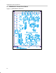
1.4 Setting Functions
All functions of the devices (PCM3010, DIR1703, DIT4096) on the
DEM-DAI3010 are controlled by DIP switches or header pins on this PCB.
Therefore, the DEM-DAI3010 does not require a microcontroller or software
to transmit data to internal function-setting registers. For specific information
on any device, see the data sheet for that device.
1.4.1 Function Setting Switches and Header Pins
Table 1–3.Switches and Header Pins of the DEM-DAI3010
SW/JP No. Item Shape
SW001 S/PDIF input selection (optical/coax) Toggle switch
SW002 Reset of DIR1703 and DIT4096 Pushbutton switch
SW003 Format and system clock setting of DIR1703 4-pole DIP switch
SW004 Output clock selection of DIR1703 (X’tal/Auto/PLL) Toggle switch
SW005 Format and system clock setting of DIT4096 4-pole DIP switch
SW006 Channel status data setting of DIT4096 10-pole DIP switch
SW051 S/PDIF output selection (optical/coax) Toggle switch
SW101 Setting of PCM3010 (format, de-emphasis, power down) 5-pole DIP switch
JP001 Crystal frequency and system clock setting of DIR1703 2×5 header
JP107 Connection of S/PDIF I/O circuit and PCM3010 2×7 header
JP101 Cutoff frequency setting of DAC output filter (L-ch) 2×2 header
JP102 Cutoff frequency setting of DAC output filter (R-ch) 2×2 header
JP103 Cutoff frequency setting of DAC output filter (L-ch) 2×1 header
JP104 Cutoff frequency setting of DAC output filter (R-ch) 2×1 header
JP105 Selection of L-ch ADC input terminal (CN101/CN103) 2×2 header
JP106 Selection of R-ch ADC input terminal (CN102/CN104) 2×2 header
CN057 The way of power supply of PCM3010 V
DD
(3.3 V) 2×1 header
Note: The relation between the DIP switch setting (ON/OFF) and the setting of the IC input port is printed on the PCB. The DIP
switch H position does not always set the IC input port level HIGH.
Toggle switch settings are printed on the PCB.