
Datasheet


www.ti.com
3 Components
Components
Components that have RF performance similar to the ones listed in Table 1 may be substituted.
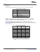
Table 1. Component Descriptions
PART DESCRIPTION
C
1
, C
2
Tantalum Chip Capacitor, SMD EIA Size 3528,
20V
C
3
, C
4
Multilayer Ceramic Chip Capacitor, SMD 1206, 50V
J
1A
– J
2B
SMA or SMB Board Jack (Amphenol 901-144-8)
L
1
, L
2
EMI-Suppression Ferrite Chip, SMD 1206 (Steward
LI 1206 B 900 R)
P
1
, P
2
Terminal Block, 3.5mm Centers (On-Shore
Technology ED555/3DS)
R
1A
– R
7B
Metal Film Chip Resistor, SMD 1206, 1/8W
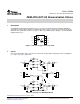
R
1
and R
7
set the I/O impedance; R
2
through R
6
set the gain; and C
1
through C
4
are supply bypass
capacitors. L
1
and L
2
are ferrite chips that can reduce interactions with the power supply at high
frequencies. If not desired, they can be replaced with 0 Ω resistors.
For single-supply operation, do not connect P
2
, L
2
and C
2
. Use a 0 Ω resistor in place of C
3
.
Voltage Feedback Amplifier Circuit Configuration—These op amps have the pinout illustrated in
Figure 1 . Table 2 lists typical values used. To select component values for a specific op amp , consult the
respective data sheet.
Table 2. Circuit Configuration
(1)
SINGLE-
DUAL-SUPPLY DUAL-SUPPLY SUPPLY
COMPONENT (G = +2) (G = –1) (G = +1)
R
1
49.9 Ω 57.6 Ω 49.9 Ω
R
2
174 Ω Open 0 Ω
R
3
Open 205 Ω Open
R
4
Open 402 Ω Open
R
5
402 Ω Open Open
R
6
402 Ω 402 Ω 24.9 Ω
R
7
49.9 Ω 49.9 Ω 49.9 Ω
C
1
2.2 µ F 2.2 µ F 2.2 µ F
C
2
2.2 µ F 2.2 µ F Open
C
3
0.1 µ F 0.1 µ F 0 Ω
C
4
0.1 µ F 0.1 µ F 0.1 µ F
(1)
The values and gains listed here will not work for all op amps. See
the specific data sheet to select proper values. The I/O impedances
are 50 Ω .
DEM-OPA-SOT-2A Demonstration Fixture2 SBOU001A – June 2000 – Revised May 2006
Submit Documentation Feedback