Data Manual 2001 Digital Audio: Digital Speakers SLAS307B
IMPORTANT NOTICE Texas Instruments and its subsidiaries (TI) reserve the right to make changes to their products or to discontinue any product or service without notice, and advise customers to obtain the latest version of relevant information to verify, before placing orders, that information being relied on is current and complete.
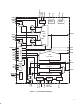
1 Introduction 1.1 Description The TAS3002 device is a system-on-a-chip that replaces conventional analog equalization to perform digital parametric equalization, dynamic range compression, and loudness contour. Additionally, this device provides high-quality, soft digital volume, bass, and treble control. All control parameters are uploaded from an outside MCU through the I2C slave port or from an external EEPROM through the I2C master port.
• Two I2C-selectable, single-ended analog input stereo channels • Equalization bypass mode • Single 3.3-V power supply • Power down without reloading the coefficients • Sampling rates of 32 kHz, 44.1 kHz, or 48 kHz • Master clock frequency of 256 fS or 512 fS • Can have crystal input to replace MCLK. Crystal input frequency is 256 fS. • Six GPI terminals for volume, bass, treble up/down control, mute, and selection of equalization filters 1.
DVSS DVDD AVSS AVDD VREFP VRFILT AVSS(REF) VREFM AINRP AINRM Voltage Reference RINA RINB Analog Supplies Digital Supplies AINRP AINRM 24-Bit Stereo ADC AINLP AINLM SDOUT0 LINA AINLP LINB AINLM VCOM ALLPASS INPA GPI4 GPI3 GPI2 AOUTL Controller GPI5 AOUTR 24-Bit Stereo DAC GPI1 GPI0 L+R SDOUT2 CS1 SDA SCL I2C Control L+R 32-Bit Audio Signal Processor PLL CAP_PLL MCLKO XTALI/ MCLK XTALO OSC/CLK Select CLKSEL IFM/S SDATA Control SCLK/O TEST 32-Bit Audio Signal Processor R L
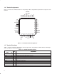
1.4 Terminal Assignments Figure 1−2 shows the terminal locations on the package outline, along with the signal name assigned to each terminal.
Table 1−1. TAS3002 Terminal Functions (Continued) TERMINAL NAME NO. I/O DESCRIPTION CAP_PLL 10 I Loop filter for internal phase-locked loop (PLL) CLKSEL 11 I CS1 7 I Logic low selects 256 fS; logic high selects 512 fS MCLK I2C address bit A0; low = 68h, high = 6Ah DVDD 17 I Digital power supply (3.
1−6
2 Audio Data Formats 2.1 Serial Interface Formats The TAS3002 device works in master or slave mode. In the master mode, terminal 21 (IFM/S) is tied high. This activates the master clock (MCLK) circuitry. A crystal can be connected across terminals 13 (XTALI/MCLK) and 14 (XTALO), or an external, TTL-compatible MCLK can be connected to XTALI/MCLK. In that case, MCLK is outputs on terminal 12 (MCLKO), with terminals 19 (LRCLK/O) and 20 (SCLK/O) becoming outputs to drive slave devices.
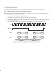
2.2 Digital Output Modes The digital output modes (SDOUT1, SDOUT2, SDOUT0) are described in Sections 2.2.1 through 2.2.3. 2.2.1 MSB-First, Right-Justified, Serial-Interface Format The normal output mode for the MSB-first, right-justified, serial-interface format is for 16, 18, 20, or 24 bits. Figure 2−1 shows the following characteristics of this protocol: • Left channel is transmitted when LRCLK is high. • The SDIN(s) (recorded) data is justified to the trailing edge of the LRCLK.
2.2.2 I2S Serial-Interface Format The normal output mode for the I2S serial-interface format is for 16, 18, 20, or 24 bits. Figure 2−2 shows the following characteristics of this protocol: • Left channel is transmitted when LRCLK is low. • SDIN is sampled with the rising edge of SCLK. • SDOUT is transmitted on the falling edge of SCLK. • If the LRCLK phase changes by more than 10 cycles of MCLK, the codec automatically resets.
2.2.3 MSB-Left-Justified, Serial-Interface Format The normal output mode for the MSB-left-justified, serial-interface format is for 16, 18, 20, or 24 bits. Figure 2−3 shows the following characteristics of this protocol: • Left channel is transmitted when LRCLK is high. • The SDIN data is justified to the leading edge of the LRCLK. • The MSBs are transmitted at the same time as LRCLK edge and captured at the next rising edge of SCLK.
2.3 Switching Characteristics PARAMETER MIN tc(SCLK) td(SLR) SCLK cycle time td(SDOUT) tsu(SDIN) SDOUT valid from SCLK falling edge (see Note 1) th(SDIN) f(LRCLK) SDIN hold after SCLK rising edge TYP MAX 325.5 SCLK rising to LRCLK edge ns 20 ns (1/256 fS) + 10 SDIN setup before SCLK rising edge 20 32 Duty cycle ns ns 100 LRCLK frequency UNIT ns 44.1 48 50 kHz % NOTE 1: Maximum of 50-pF external load on SDOUT.
2−6
3 Analog Input/Output The TAS3002 device contains a stereo 24-bit ADC with two single-ended inputs per channel. Selection of the A or B analog input is accomplished by setting a bit in the analog control register (ACR) by an I2C command. Additionally, the TAS3002 device has a stereo 24-bit digital-to-analog converter (DAC). 3.1 Analog Input Figure 3−1 shows the technique and components required for analog input to the TAS3002 device. The maximum input signal must not exceed 0.7 Vrms.
Analog Output (Adjust Capacitors for Desired Low Frequency Response) AOUTR 24-Bit DAC VCOM + 10 µF AOUTL 0.1 µF AGND Figure 3−2. VCOM Decoupling Network 3.2.2 Analog Output With Gain Because the maximum analog output from the TAS3002 device is 0.707 Vrms, the output level can be increased by using an external amplifier. The circuit shown in Figure 3−3 boosts the output level to 1 Vrms (when it has a gain of 1.414) and provides improved signal-to-noise ratio (SNR).
3.2.3 Reference Voltage Filter Figure 3−4 shows the TAS3002 reference voltage filter. 0.1 µF 4 3 2 45 VREFM 0.1 µF VRFILT 0.1 µF AVSS(REF) 1 µF + AVSS 15 µF + VREFP 44 TAS3002 Figure 3−4.
3−4
4 Audio Control/Enhancement Functions 4.1 Soft Volume Update The TAS3002 device implements a TI proprietary soft volume update. This feature allows a smooth and pleasant-sounding change from one volume level to another over the entire range of volume control (18 dB to mute). The volume is adjustable by downloading a gain coefficient through the I2C interface in 4.16 format—4 bits for the integer and 16 bits for the fractional part. NO TAG lists the 4.
Left Channel Mix Coefficients I2C Register Address 08h SDIN1 ^ SDIN2 ^ ADC = (3) 24-Bit Left Mix Coefficient SDIN1_L SDIN2_L L_SUM 7 Biquad Filters Tone Soft Volume DRCE ADC_L SDOUT1 SDIN1_R SDIN2_R 7 Biquad Filters Tone Soft Volume DRCE ADC_R R_SUM 1/2 L + R_SUM SDOUT2 1/2 Right Channel Mix Coefficients I2C Register Address 07h SDIN1 ^ SDIN2 ^ ADC = (3) 24-Bit Right Mix Coefficient Figure 4−1. TAS3002 Mixer Function 4.
4.6 Bass Control The bass gain level can be adjusted within the range of 15 dB to −15 dB with 0.5-dB step resolution. The level changes are accomplished by downloading bass codes (shown in NO TAG) into the bass frequency control register. Alternatively, a limited range of bass control is available by asserting the bass-up or bass-down GPI terminal (see Section 7.6.1). Bass control is a shelf filter with a corner frequency of 250 Hz at a 48-kHz sample rate.
4.8 Analog Control Register (40h) The analog control register (ACR) allows control of de-emphasis, selection of the analog input channel to the ADC, and analog power down. An I2C master is required to write the appropriate command into the ACR. The ACR subaddress is 40h. Bit Type Default 7 6 5 4 3 2 1 0 R/W R/W R/W R/W R/W R/W R/W R/W 0 0 0 0 0 0 0 0 Table 4−1.
4.9 Dynamic Loudness Contour The necessity for applying loudness compensation to playback systems to compensate for the fact that the ear perceives bass and treble less audibly at low levels than at high ones has been established since the first data was published by Fletcher and Munson in 1933. There are many equal-loudness contours in publication, like Steven’s contours, Robinson and Dadson contours. Some have even reached the acceptance level of ISO recommendation.
4.10 Dynamic Range Compression/Expansion (DRCE) The TAS3002 device provides the user with the ability to manage the dynamic range of the audio system. The DRCE receives data, and affects scaling after the volume/loudness block. As shown in Figure 4−4, the DRCE is applied after the volume/loudness control block as a DRCE scale factor. The DRCE must be adjusted such that the signal does not reach the hard limit value.
4.12 Main Control Register 1 (01h) The TAS3002 device contains two main control registers: main control register 1 (MCR1) and main control register 2 (MCR2). The MCR1 register contains the bits associated with load speed, SCLK frequency, serial-port mode, and serial-port word length. It is accessed via I2C with the address 01h. MCR1 (01h) Bit Type Default b7 b6 b5 b4 b3 b2 b1 b0 R/W R/W R/W R/W R R R/W R/W 1 X X X X X X X Table 4−2.
4−8
5 Filter Processor 5.1 Biquad Block The biquad block consists of seven digital biquad filters per channel organized in a cascade structure, as shown in Figure 5−1. Each of these biquad filters has five downloadable 24-bit (4.20) coefficients. Each stereo channel has independent coefficients. Biquad 0 Biquad 1 ... Biquad 6 Figure 5−1. Biquad Cascade Configuration 5.1.
5−2
6 I2C Serial Control Interface 6.1 Introduction Control parameters for the TAS3002 device can be loaded from an I2C serial EEPROM by using the TAS3002 master interface mode. If no EEPROM is found, the TAS3002 device becomes a slave device and loads from another I2C master interface. Information loaded into the TAS3002 registers is defined in Appendix A. The I2C bus uses terminals 16 (SDA for data) and 15 (SCL for clock) to communicate between integrated circuits in a system.
Table 6−1 lists the definitions used by the I2C protocol. Table 6−1. I2C Protocol Definitions DEFINITION DESCRIPTION Transmitter The device that sends data Receiver The device that receives data Master The device that initiates a transfer, generates clock signals, and terminates the transfer Slave The device addressed by the master Multimaster More than one master can attempt to control the bus at the same time without corrupting the message.
TAS3002 I2C Readback Example 6.3.2 The TAS3002 saves in a stack or first-in first-out (FIFO) buffer the last 7 bytes that were sent to it. When an I2C read command is sent to the device (LSB=high), it answers by popping the first byte off the stack. The TAS3002 then expects either a Send Ack command or an I2C Stop command from the host. If a Send Ack command is sent from the host then the TAS3002 pops another byte off the stack. If an I2C Stop is sent then the TAS3002 ends this transaction.
Table 6−3 gives typical values of the wait states that can be expected with the various functions of the part: Table 6−3. I2C Wait States SYSTEM SAMPLING FREQUENCY Comment 32 kHz 44.1 kHz 48 kHz Volume 62 ms 49 ms 41 ms Not dependent on size of change Bass 231 ms 167 ms 153 ms 0 to −18 dB Treble 231 ms 167 ms 153 ms 0 to −18 dB DRC on 300 µs 300 µs 300 µs Mixer None None None Loudness None None None Equalization 15 ms 190 µs 300 µs Can occur with each filter 6.
6.4.3 Wait States If separate I2C/SMBus commands are sent too frequently, the TAS3002 device can generate a bus wait state. This happens when the device is busy while performing smoothing operations and changing volume, bass, and treble. The wait occurs after the bus acknowledge on the first data byte and can exceed the maximum allowable time allowed according to the SMBus specification (worst case 200 ms).
6−6
7 Microcontroller Operation The TAS3002 device contains an internal microcontroller programmed by Texas Instruments to perform housekeeping and interface functions. Additionally, it handles I2C communication and general purpose input functions. 7.1 General Description The microcontroller uses a 256fS system clock and can access up to 8K bytes of memory. It interfaces with the digital audio interface I2C master/slave for downloading data and coefficients.
• Clears all the registers in the circuits • Purges the codec • Selects analog input A (RINA and LINA) and sets the input A active indicator (INPA) low • Initializes the equalization parameters to AllPass filters • Sets the digital audio interface to the I2S 18-bit mode • Sets the bass/treble to 0 dB • Sets the mixer gain to 0 dB SDIN1 and mutes both SDIN2 and analog-in • Sets the volume to –40 dB • Turns off all enhancement features (DRCE, etc.) • Reads the I2C address.
Bass and treble cannot download in this mode. Mixer1 and Mixer2 registers can download in this mode or normal mode (FL bit = 0). Once the download is complete, the fast load bit must be cleared by writing a 0 into bit 7 of main control register 1 (MCR1). This puts the TAS3002 device into normal mode. 7.2.5 Codec Reset During initialization, the output of the codec is disabled. Throughout reset and initialization, the output of the DAC is muted to prevent extraneous noise being sent to the system output.
7.3.1 Power-Down Timing Sequence PWR_DN RESET MCLK SCLK LRCLK SDATA Power-Down Mode Normal Operation 1 ms Figure 7−2. Power-Down Timing Sequence In power-down mode, the TAS3002 device typically consumes less than 1 mA. 7.4 Test Mode Terminal 9 (TEST) is tied low in normal operation. This function is reserved for factory test and must not be asserted. 7.5 Internal Interface Figure 7−3 shows the flow chart of the interface between the microcontroller and its peripheral blocks. 7.
Table 7−1. GPI Terminal Programming GPI5 VOL_UP, +1 dB GPI4 GPI3 GPI2 GPI1 x VOL_DN, −1 dB x BASS_UP, +1 dB x BASS_DN, −1 dB x TREB_UP, +1 dB x TREB_DN, −1 dB x Shift 1 x Mute x EQ1 GPI0 x x EQ2 x EQ3 x EQ4 x EQ5 x Shift 2 x x NOTE: x = Logic low Initially (after reset), the TAS3002 GPI is set to control volume, bass, and treble. Simultaneously setting GPI bits 1 and 5 low for 1 second changes the function of the GPI terminals to control mute and equalization.
Start Power Up Restore Volume and MCR Initialize Default EEPROM Initialize TAS3002 TAS3001 Slave Write Load Parameters and Coefficients to DSP GPI Power Down Volume/Bass/Treble Up/Down Echo to TAS3001 Switch BQ Set Save Volume, Mute Save PWR_DN Stop PLL Stop DRC_OFF DRC Figure 7−3.
7.7 External EEPROM Memory Maps Table 7−2 through Table 7−5 show the 512-byte and 2048-byte EEPROM memory maps. Table 7−2. 512-Byte EEPROM Memory Map 2.
Table 7−3. 512-Byte EEPROM Memory Map 2.
Table 7−4. 2048-Byte EEPROM Memory Map—2.
Table 7−5. 2048-Byte EEPROM Memory Map—2.
8 Electrical Characteristics 8.1 Absolute Maximum Ratings Over Operating Temperature Ranges† Supply voltage range: AVDD . . . . . . . . . . . . . . . . . . . . . . . . . . . . . . . . . . . . . . . . . . . . . . . . . . . . . . −0.3 V to 3.6 V DVDD . . . . . . . . . . . . . . . . . . . . . . . . . . . . . . . . . . . . . . . . . . . . . . . . . . . . . . −0.3 V to 3.6 V Analog input voltage range: . . . . . . . . . . . . . . . . . . . . . . . . . . . . . . . . . . . . . . . . . . . . . . . . . . −0.
8.4 ADC Digital Filter TA = 25°C, AVDD = 3.3 V, DVDD = 3.3 V, fS = 48 kHz, 20-bit I2S mode All terms characterized by frequency are scaled with the chosen sampling frequency, fS. See Figure 8−1 through Figure 8−4 for performance curves of the ADC digital filter. PARAMETER ADC decimation filter (LPF) TEST CONDITIONS Pass band MIN 0.0 dB kHz 80 dB 720 20 Hz to 20 kHz Hz 1.23 degrees Amplitude − dB 0 −50 −100 −150 −200 2 fs 4 fs 6 fs f − Frequency − Hz 8 fs 10 fs 12 fs Figure 8−1.
0.008 Amplitude − dB 0.006 0.004 0.002 0 −0.002 0 0.1 fs 0.2 fs 0.3 fs f − Frequency − Hz 0.4 fs 0.5 fs Figure 8−3. ADC Digital Filter Pass-Band Characteristics 0.2 Amplitude − dB 0 −0.2 −0.4 −0.6 −0.8 −1 0 1 fs 2 fs f − Frequency − Hz 3 fs 4 fs Figure 8−4. ADC High-Pass Filter Characteristics 8.5 Analog-to-Digital Converter TA = 25°C, AVDD = 3.3 V, DVDD = 3.3 V, fS = 48 kHz, 20-bit I2S mode All terms characterized by frequency are scaled with the chosen sampling frequency, fS.
8.6 Input Multiplexer TA = 25°C, AVDD = 3.3 V, DVDD = 3.3 V, fS = 48 kHz, 20-bit I2S mode PARAMETER TEST CONDITIONS MIN TYP MAX UNIT Input impedance 20 Crosstalk 85 kΩ dB Full-scale input voltage range 1.7 VPP 8.7 DAC Interpolation Filter TA = 25°C, AVDD = 3.3 V, DVDD = 3.3 V, fS = 48 kHz, 20-bit I2S mode All terms characterized by frequency are scaled with the normal mode sampling frequency, fS. See Figure 8−5 and Figure 8−6 for performance curves of the DAC digital filter.
8.8 Digital-to-Analog Converter TA = 25°C, AVDD = 3.3 V, DVDD = 3.3 V, fS = 48 kHz, input = 0 dB-fS sine wave at 1 kHz PARAMETER TEST CONDITIONS MIN TYP MAX UNIT SNR (EIAJ) A weighted 94 99 dB Dynamic range −60 dB, 1 kHz 92 96 dB Signal to (noise + distortion) ratio 0 dB, 1 kHz, 20 Hz to 20 kHz 83 dB Power supply rejection ratio 1 kHz 50 dB +118 dB Idle channel tone rejection Intermodulation distortion −75 Frequency response −0.5 Deviation from linear phase dB +0.5 dB ±1.
8.10 I2C Serial Port Timing Characteristics MIN MAX UNIT 0 100 kHz f(SCL) t(buf) SCL clock frequency Bus free time between start and stop 4.7 µs t(low) t(high) Low period of SCL clock 4.7 µs High period of SCL clock 4.0 µs th(sta) Hold time repeated start tsu(sta) Setup time repeated start 4.0 4.
9 System Diagrams Figure 9−1 and Figure 9−2 show the TAS3002 stereo and 2.1-channel applications, respectively. +3.3 VDD Analog In SPDIF or USB EEPROM I2S I2C Clock Select Logic RESET Analog Out TAS3002 Master B-T-V-EQ Switches NOTE: Items such as the PLL network and power supplies are omitted for clarity. Figure 9−1.
+3.3 VDD Analog In SPDIF or USB EEPROM Echoes Switches on GPIO I2S I2C Clock Select Logic RESET Master Analog Out (To Satellite Amplifiers) TAS3002 SDOUT2 I2S_OUT B-T-V-EQ-Sub Vol L+R Mix I2C Slave I2S PCM1744 TAS3001 Address = 6Ah NOTE: Items such as the PLL network and power supplies are omitted for clarity. Figure 9−2. TAS3002 Device, 2.
10 Mechanical Information The TAS3002 device is packaged in a 48-terminal PFB package. The following illustration shows the mechanical dimensions for the PFB package. PFB (S-PQFP-G48) PLASTIC QUAD FLATPACK 0,27 0,17 0,50 36 0,08 M 25 37 24 48 13 0,13 NOM 1 12 5,50 TYP 7,20 SQ 6,80 9,20 SQ 8,80 Gage Plane 0,25 0,05 MIN 0°−ā 7° 1,05 0,95 Seating Plane 1,20 MAX 0,75 0,45 0,08 4073176 / B 10/96 NOTES: A. All linear dimensions are in millimeters. B.
10−2