
Network Router User Manual
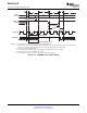
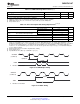
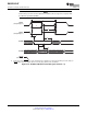

PWM
(see Note C)
TxCTRIP
, CxTRIP,
PDPINTx
(see Note B)
XCLKOUT
(see Note A)
t
w(PDP)
, t
w(CxTRIP)
, t
w(TxCTRIP)
t
d(PDP-PWM)HZ
, t
d(TRIP-PWM)HZ
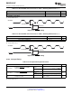
XNMI, XINT1, XINT2
t
w(INT)
Interrupt Vector
t
d(INT)
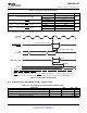
A0−A15
SM320F2812-HT
www.ti.com
SGUS062A–JUNE 2009–REVISED APRIL 2010
Table 6-18. Interrupt Timing Requirements
MIN MAX UNIT
with no qualifier 2 × t
c(SCO)
t
w(INT)
(1)
Pulse duration, INT input low/high cycles
with qualifier 1 × t
c(SCO)
+ IQT
(2)
with no qualifier 2 × t
c(SCO)
t
w(PDP)
Pulse duration, PDPINTx input low cycles
with qualifier 1 × t
c(SCO)
+ IQT
(2)
with no qualifier 2 × t
c(SCO)
t
w(CxTRIP)
(1)
Pulse duration, CxTRIP input low cycles
with qualifier 1 × t
c(SCO)
+ IQT
(2)
with no qualifier 2 × t
c(SCO)
t
w(TxCTRIP)
(1)
Pulse duration, TxCTRIP input low cycles
with qualifier 1 × t
c(SCO)
+ IQT
(2)
(1) Not production tested.
(2) Input Qualification Time (IQT) = [5 × QUALPRD × 2] × t
c(SCO)
A. XCLKOUT = SYSCLKOUT
B. TxCTRIP – T1CTRIP, T2CTRIP, T3CTRIP, T4CTRIP . CxTRIP – C1TRIP, C2TRIP, C3TRIP, C4TRIP, C5TRIP, or
C6TRIP. PDPINTx – PDPINTA or PDPINTB
C. PWM refers to all the PWM pins in the device (i.e., PWMn and TnPWM pins or PWM pin pair relevant to each
CxTRIP pin). The state of the PWM pins after PDPINTx is taken high depends on the state of the FCOMPOE bit.
Figure 6-20. External Interrupt Timing
6.17 General-Purpose Input/Output (GPIO) – Output Timing
Table 6-19. General-Purpose Output Switching Characteristics
PARAMETER MIN MAX UNIT
t
d(XCOH-GPO)
Delay time, XCLKOUT high to GPIO low/high All GPIOs 1 × t
c(SCO)
cycle
t
r(GPO)
(1)
Rise time, GPIO switching low to high All GPIOs 10 ns
t
f(GPO)
(1)
Fall time, GPIO switching high to low All GPIOs 10 ns
f
GPO
(1)
Toggling frequency, GPO pins 20 MHz
(1) Not production tested.
Copyright © 2009–2010, Texas Instruments Incorporated Electrical Specifications 107
Submit Documentation Feedback
Product Folder Link(s): SM320F2812-HT