
Network Router User Manual
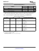

ac
R
s
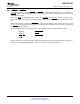
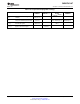
ADCIN0
C
p
10 pF
R
on
1 kΩ
1.25 pF
C
h
Switch
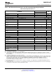
Typical Values of the Input Circuit Components:
Switch Resistance (R
on
): 1 kΩ
Sampling Capacitor (C
h
): 1.25 pF
Parasitic Capacitance (C
p
): 10 pF
Source Resistance (R
s
): 50 Ω
28x DSP
Source
Signal
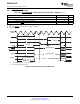
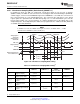
ADC Power Up Delay
ADC Ready for Conversions
PWDNBG
PWDNREF
PWDNADC
Request for
ADC
Conversion
t
d(BGR)
t
d(PWD)
SM320F2812-HT
www.ti.com
SGUS062A–JUNE 2009–REVISED APRIL 2010
Figure 6-37. ADC Analog Input Impedance Model
6.29.4 ADC Power-Up Control Bit Timing
Figure 6-38. ADC Power-Up Control Bit Timing
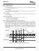
Table 6-49. ADC Power-Up Delays
(1) (2)
MIN TYP MAX UNIT
Delay time for band gap reference to be stable. Bits 6 and 5 of the ADCTRL3 register
t
d(BGR)
7 8 10 ms
(PWDNBG and PWDNREF) are to be set to 1 before the ADCPWDN bit is enabled.
20 50 ms
Delay time for power-down control to be stable. Bit 7 of the ADCTRL3 register (ADCPWDN)
t
d(PWD)
is to be set to 1 before any ADC conversions are initiated.
1 ms
(1) These delays are necessary and recommended to make the ADC analog reference circuit stable before conversions are initiated. If
conversions are started without these delays, the ADC results shows a higher gain. For power down, all three bits can be cleared at the
same time.
(2) Not production tested.
Copyright © 2009–2010, Texas Instruments Incorporated Electrical Specifications 137
Submit Documentation Feedback
Product Folder Link(s): SM320F2812-HT