
Network Router User Manual
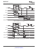
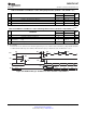
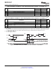
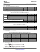

Bit 0 Bit(n-1) (n-2) (n-3) (n-4)
Bit 0 Bit(n-1) (n-2) (n-3) (n-4)
CLKX
FSX
DX
DR
M54
M58
M56
M53
M55
M59
M57
LSB
MSB
M60
M61
SM320F2812-HT
SGUS062A–JUNE 2009 –REVISED APRIL 2010
www.ti.com
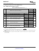
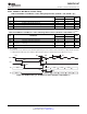
Table 6-60. McBSP as SPI Master or Slave Timing Requirements (CLKSTP = 11b, CLKXP = 1)
(1)
MASTER SLAVE
NO. UNIT
MIN MAX MIN MAX
M58 t
su(DRV-CKXL)
Setup time, DR valid before CLKX low P – 10 8P – 10 ns
M59 t
h(CKXL-DRV)
Hold time, DR valid after CLKX low P – 10 8P – 10 ns
M60 t
su(FXL-CKXL)
Setup time, FSX low before CLKX low 16P + 10 ns
M61 t
c(CKX)
Cycle time, CLKX 2P 16P ns
(1) Not production tested.
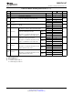
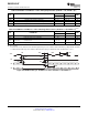
Table 6-61. McBSP as SPI Master or Slave Switching Characteristics (CLKSTP = 11b, CLKXP = 1)
(1) (2)
MASTER
(3)
SLAVE
NO. PARAMETER UNIT
MIN MAX MIN MAX
M53 t
h(CKXH-FXL)
Hold time, FSX low after CLKX high P ns
M54 t
d(FXL-CKXL)
Delay time, FSX low to CLKX low 2P ns
Disable time, DX high impedance following last data bit from CLKX
M56 t
dis(CKXH-DXHZ)
P + 6 7P + 6 ns
high
M57 t
d(FXL-DXV)
Delay time, FSX low to DX valid 6 4P + 6 ns
(1) Not production tested.
(2) 2P = 1/CLKG
For all SPI slave modes, CLKX has to be minimum eight CLKG cycles. Also, CLKG should be LSPCLK/2 by setting CLKSM = CLKGDV
= 1. With maximum LSPCLK speed of 75 MHz, CLKX maximum frequency is LSPCLK/16, that is 4.5 MHz and P = 13.3 ns.
(3) C = CLKX low pulse width = P
D = CLKX high pulse width = P
Figure 6-46. McBSP Timing as SPI Master or Slave: CLKSTP = 11b, CLKXP = 1
148 Electrical Specifications Copyright © 2009–2010, Texas Instruments Incorporated
Submit Documentation Feedback
Product Folder Link(s): SM320F2812-HT