
Network Router User Manual


SM320F2812-HT
www.ti.com
SGUS062A–JUNE 2009–REVISED APRIL 2010
6.31 Flash Timing
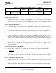
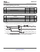
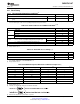
6.31.1 Recommended Operating Conditions
(4)
MIN NOM MAX UNIT
N
f
Flash endurance for the array (Write/erase cycles) 0°C to 85°C 100 1000 cycles
Maximum One-Time Programmable (OTP) endurance for the array (Write
N
OTP
0°C to 85°C 1 write
cycles)
(4) Flash Timing Endurance is the minimum number of write/erase or write cycles specified over a programming temperature range of 0°C
to 85°C. Flash may be read over the operating temperature range of the device.
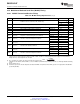
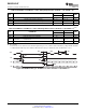
Table 6-62. Flash Parameters at 150-MHz SYSCLKOUT
(1) (2)
PARAMETER MIN TYP MAX UNIT
16-Bit Word 35 ms
Program
8K Sector 170 ms
Time
16K Sector 320 ms
8K Sector 10 s
Erase Time
16K Sector 11 s
Erase 75 mA
I
DD3VFLP
V
DD3VFL
current consumption during the Erase/Program cycle
Program 35 mA
I
DDP
V
DD
current consumption during Erase/Program cycle 140 mA
I
DDIOP
V
DDIO
current consumption during Erase/Program cycle 20 mA
(1) Typical parameters as seen at room temperature using flash API V1 including function call overhead.
(2) Not production tested.
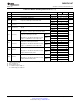
Table 6-63. Flash/OTP Access Timing
(1) (2)
PARAMETER MIN TYP MAX UNIT
t
a(fp)
Paged Flash access time 36 ns
t
a(fr)
Random Flash access time 36 ns
t
a(OTP)
OTP access time 60 ns
(1) For 150 MHz, PAGE WS = 5 and RANDOM WS = 5
For 135 MHz, PAGE WS = 4 and RANDOM WS = 4
(2) Not production tested.
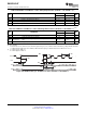
Table 6-64. Minimum Required Wait-States at Different Frequencies
(1)
SYSCLKOUT (MHz) SYSCLKOUT (ns) PAGE WAIT-STATE
(2)
RANDOM WAIT STATE
(2) (3)
150 6.67 5 5
120 8.33 4 4
100 10 3 3
75 13.33 2 2
50 20 1 1
30 33.33 1 1
25 40 0 1
15 66.67 0 1
(1) Not production tested.
(2) Formulas to compute page wait state and random wait state:
(3) Random wait state must be greater than or equal to 1
Copyright © 2009–2010, Texas Instruments Incorporated Electrical Specifications 149
Submit Documentation Feedback
Product Folder Link(s): SM320F2812-HT