
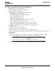
Network Router User Manual
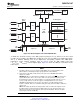
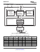
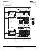

ADCINA[7:0]
ADCINB[7:0]
ADCLO
ADCBGREFIN
ADC External Current Bias Resistor ADCRESEXT
ADCREFP
V
DDA1
V
DDA2
V
SSA1
V
SSA2
AVDDREFBG
AVSSREFBG
V
DDAIO
V
SSAIO
V
DD1
V
SS1
Test Pin
ADC Reference Positive Input
ADCREFMADC Reference Medium Input
ADC Analog Power
ADC Reference Power
ADC Analog I/O Power
ADC Digital Power
Analog Input 0−3 V With Respect to ADCLO
Connect to Analog Ground
24.9 k20 k (See Note C)
Analog 3.3 V
Analog 3.3 V
Analog 3.3 V
Analog 3.3 V
Analog Ground
1.8 V Can use the same 1.8-V (or 1.9-V)
supply as the digital core but separate the
two with a ferrite bead or a filter
Digital Ground
ADC 16-Channel Analog Inputs
1 F −10 F
2 V
1 V
1 F − 10 F
NOTES: A. External decoupling capacitors are recommended on all power pins.
B. Analog inputs must be driven from an operational amplifier that does not degrade the ADC performance.
C. Use 24.9 kΩ for ADC clock range 1 − 18.75 MHz; use 20 kΩ for ADC clock range 18.75 − 25 MHz.
D. It is recommended that buffered external references be provided with a voltage difference of (ADCREFP−ADCREFM)
= 1 V $ 0.1% or better.
External reference is enabled using bit 8 in the ADCTRL3 Register at ADC power up. In this mode, the accuracy of
external reference is critical for overall gain. The voltage ADCREFP−ADCREFM determines the overall accuracy. Do
not enable internal references when external references are connected to ADCREFP and ADCREFM. See the
TMS320x281x DSP Analog-to-Digital Converter (ADC) Reference Guide (literature number SPRU060) for more
information.
(See
Note D)
SM320F2812-HT
www.ti.com
SGUS062A–JUNE 2009–REVISED APRIL 2010
Figure 4-6. ADC Pin Connections With External Reference
Copyright © 2009–2010, Texas Instruments Incorporated Peripherals 63
Submit Documentation Feedback
Product Folder Link(s): SM320F2812-HT