
Datasheet


DIT4096
10
SBOS225A
www.ti.com
LINE DRIVER OUTPUTS
The DIT4096 includes a balanced line driver. The line driver
outputs are TX– (pin 17) and TX+ (pin 18). In Software mode,
the line driver input is taken from either the output of the on-
chip AES-3 encoder, or from an external AES-3 encoded
source input at RXP (pin 9). The input source is selected
using the BYPASS bit in control register 01
H
(defaults to the
on-chip AES-3 encoder). In Hardware mode, the line driver
source is always the on-chip AES-3 encoder.
The outputs of the line driver will follow the AES-3 encoded
data source in normal operation. During a hardware or
software reset, or when the device is in power-down mode,
the line driver outputs will be forced to ground. The outputs
can also be forced to ground at any time in Software mode
by setting the TXOFF bit to 1 in control register 01
H
.
CONTROL PORT OPERATION
(SOFTWARE MODE ONLY)
For Software mode operation, the DIT4096 includes a serial
control port, which is used to write and read control registers
and the channel status data buffer. Port signals include
CS
(pin 5), CDIN (pin 4), CDOUT (pin 2), and CCLK (pin 3).
CS
is the active low chip select. This signal must be driven
low in order to write or read control registers and the channel
status data buffer.
CDIN is the serial data input, while CDOUT serves as the
serial data output. The CDOUT pin is a tri-state output, which
is set to a high-impedance state when not performing a Read
operation, or when
CS
= 1.
CCLK is the data clock for the serial control interface. Data
is clocked in at CDIN on the rising edge of CCLK, while data
is clocked out at CDOUT on the falling edge of CCLK. Data
is clocked MSB first for both CDIN and CDOUT.
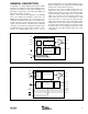
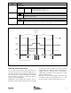
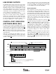
WRITE OPERATION
Figure 6 illustrates the write operation for the control port.
You may write one register or buffer address at a time, or use
the auto-increment capability built into the control port to
perform block writes. The register or buffer data is preceded
by a 16-bit header, with the first byte being used to configure
control port operation and set the starting register or buffer
address. The second byte of the header is comprised of
“don’t care” bits, which can be set to either 0 or 1 without
affecting port operation.
The first byte of the header contains two control bits, R/W
and STEP, followed by a 6-bit address. For write operations,
R/W
= 0. The STEP bit determines the address step size for
the auto-increment operation. When STEP = 0, the address
is incremented by 1. When STEP = 1, the address is
incremented by 2. Incrementing by 1 is useful when writing
multiple control registers in sequence, or when writing both left
and right channel status data in sequence. Incrementing by 2
is useful when writing just one channel of status data in
sequence.
The third byte contains the 8-bit data for the register or buffer
address designated by the first byte of the header. To write a
single address location,
CS
is brought high after the least
significant bit of the third byte is clocked into the port. For auto
increment mode,
CS
is kept low to write successive register
or buffer addresses.
Byte 0 Byte 1 Byte 2 Byte 3 Byte N
Register or Buffer Data
Header
Set CS = 1 here to write one register or buffer location.
Keep CS = 0 to enable auto-increment mode.
CS
CDIN
CCLK
R/WSTEPA5A4 A3A2A1A0
MSB LSB
BYTE 0:
BYTE DEFINITION
Auto-Increment Address Step Size: 0 = Increment Address by 1
1 = Increment Address by 2
Register or Buffer Address
Read/Write Control: Set to 1 for Read Operation
Byte 1: All 8 bits are Don’t Care. Set 0 or 1.
Bytes 2 through N: 8-Bit Register or Buffer data.
FIGURE 6. Write Operation Format.