
Datasheet


DIT4096
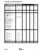
5
SBOS225A
www.ti.com
GENERAL DESCRIPTION
The DIT4096 is a complete digital audio transmitter, suitable
for both professional and consumer audio applications. Sam-
pling rates up to 96kHz are supported. The DIT4096 com-
plies with the requirements for the AES-3, IEC-60958, and
EIAJ CP1201 interface standards.
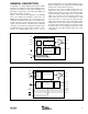
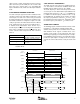
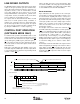
Figures 1 and 2 show the block diagrams for the DIT4096
when used in Software and Hardware control modes. The
MODE input (pin 28) determines the control model used to
configure the DIT4096 internal functions. In Software mode,
a serial control port is used to write and read on-chip control
registers and status buffers. In Hardware mode, dedicated
control pins are provided for configuration and status inputs.
The DIT4096 includes an audio serial port, which is used to
interface to standard digital audio sources, such as
Audio
Serial
Port
AES-3 Encoder
Line
Driver
Reset
Logic
Serial Control Interface,
Control Registers,
and Channel Status
Data Buffers
Clock
Generator
RXP
TX+
TX–
MCLK
U
SYNC
SCLK
SDATA
RST
Control Port
BLS
INT
Audio
Serial
Port
AES-3 Encoder
Line
Driver
Reset
Logic
CUV
Data Buffer
Clock
Generator
TX+
TX–
MCLK
CLK1
BLSM
BLS
MONO
MDAT
CLK0
SYNC
SCLK
SDATA
M/S
FMT0
FMT1
CSS
COPY/C
L
AUDIO
EMPH
U
V
RST
Analog-to-Digital (A/D) converters, Digital Signal Processors
(DSPs), and audio decoders. Support for Left-Justified, Right-
Justified, and I
2
S data formats is provided.
The AES-3 encoder creates a multiplexed bit stream, con-
taining audio, status, and user data. See Figure 3 for the
multiplexed data format. The data is then Bi-Phase Mark
encoded and output to a differential line driver. The line driver
outputs are connected to the transmission medium, be it
cable or fiber optics. In the case of twisted-pair or coaxial
cable, a transformer is commonly used to couple the driver
outputs to the transmission line. This provides both isolation
and improved common-mode rejection. For optical transmis-
sion, the TX+ (pin 18) driver output is connected to an optical
transmitter module. See the Applications Information section
of this data sheet for details regarding output driver circuit
configurations.
FIGURE 1. Software Mode Block Diagram.
FIGURE 2. Hardware Mode Block Diagram.