
Datasheet


DIT4096
6
SBOS225A
www.ti.com
MASTER CLOCK
The DIT4096 requires a master clock for operation. This
clock must be supplied at the MCLK input (pin 6). The
maximum master clock frequency that may be supplied to
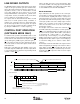
MCLK is 25MHz. Table I shows master clock rates for
common input sampling frequencies.
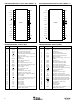
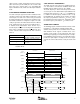
Channel AX XYYZ Channel A Channel A Channel BChannel BChannel B
Frame 191 Frame 0 Frame 1
Start of Channel Status Block
One Sub-Frame
Preamble Aux Data LSB MSB V U C P
27 28 29 30 31
Audio Data
Validity Data
User Data
Parity Bit
Channel Status Data
Bits: 0 3 4 7 8
FIGURE 3. AES-3 Frame Format.
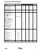
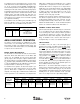
MASTER CLOCK FREQUENCY (MHz)
256 • f
S
384 • f
S
512 • f
S
SAMPLING
FREQUENCY (kHz)
22.05 5.6448 8.4672 11.2896
24 6.144 9.216 12.288
32 8.192 12.288 16.384
44.1 11.2896 16.9344 22.5792
48 12.288 18.432 24.576
88.2 22.5792 n/a n/a
96 24.576 n/a n/a
TABLE I. Master Clock Frequencies for Common Sampling Rates.
For Software mode, the master clock frequency selection is
programmed using the CLK0 and CLK1 bits in Control
Register 02
H
. For Hardware mode, the CLK0 (pin 5) and
CLK1 (pin 4) inputs are used to select the master clock
frequency. Table II shows the available MCLK frequency
selections.
RESET AND POWER-DOWN
OPERATION
The DIT4096 includes a reset input,
RST
(pin 15), which is
used to force a reset sequence. When the DIT4096 is first
powered up, the user must assert
RST
low, in order to start
the reset sequence. The
RST
input must be low for a mini-
mum of 500ns. The
RST
input is then forced high to enable
normal operation. For software mode, the reset sequence will
force all internal registers to their default settings. In addition,
the reset sequence will force all channel status bits to 0 in
Software mode.
While the
RST
input is low, the transmitter outputs,
TX– (pin 17) and TX+ (pin 18), are forced to ground.
Upon setting
RST
high, the TX– and TX+ outputs will remain
low until the rising edge of the SYNC clock is detected at
pin 12. Once this occurs, the TX– and TX+ outputs will
become active and be driven by the output of the AES-3
encoder.
In Software mode, the DIT4096 also includes software reset
and power-down bits, located in control register 02
H
. The
software reset bit,
RST
, and the software power-down bit,
PDN, are both active high.
AUDIO SERIAL PORT
The audio serial port is a 3-wire interface used to connect the
DIT4096 to an audio source, such as an A/D converter or
DSP. The port supports sampling frequencies up to 96kHz.
The port signals include SDATA (pin 13), SYNC (pin 12), and
SCLK (pin 11). The SDATA pin is the serial data input for the
port. The SCLK pin may be either an input or output, and is
used to clock serial data into the port. The SYNC pin may be
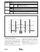
CONTROL BITS OR INPUT PINS
CLK1 CLK0
MASTER CLOCK (MCLK) SELECTION
0 0 Unused
0 1 256 • f
S
1 0 384 • f
S
1 1 512 • f
S
TABLE II. Master Clock Rate Selection for Software and
Hardware Modes.