
Datasheet

www.ti.com
GENERAL-PURPOSE DIGITAL OUTPUTS
HOST INTERFACE OPERATION:
DIX4192
SBFS031C – JANUARY 2006 – REVISED JUNE 2006
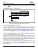
PRODUCT OVERVIEW (continued)
The DIX4192 includes four general-purpose digital outputs, GPO1 through GPO4 (pins 26 through 29,
respectively). A GPO pin may be programmed to a static high or low state. Alternatively, a GPO pin may be
connected to one of 13 internal logic nodes, allowing the GPO pin to inherit the function of the selected signal.
Control registers 0x1B through 0x1E are utilized to select the function of the GPO pins. For details regarding
GPO output configuration, refer to the Control Registers section. Table 1 summarizes the available output
options for the GPO pins.
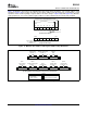
Table 1. General-Purpose Output Pin Configurations
GPOn3 GPOn2 GPOn1 GPOn0 GPOn FUNCTION
0 0 0 0 GPOn is forced low (default)
0 0 0 1 GPOn is forced high
0 0 1 0 Reserved
0 0 1 1 DIT interrupt flag; active low
0 1 0 0 DIR interrupt flag; active low
0 1 0 1 DIR 50/15 µ s emphasis flag; active low
0 1 1 0 DIR non-audio data flag; active high
0 1 1 1 DIR non-valid data flag; active high
1 0 0 0 DIR channel status data serial output
1 0 0 1 DIR user data serial output
1 0 1 0 DIR block start clock output
DIR COPY bit output
1 0 1 1
(0 = copyright asserted, 1 = copyright not asserted)
DIR L (or origination) bit output
1 1 0 0
(0 = 1st generation or higher, 1 = original)
1 1 0 1 DIR Parity error flag; active high
DIR internal sync clock output; may be used as the data clock for the channel
1 1 1 0
status and user data serial outputs.
1 1 1 1 DIT internal sync clock
SERIAL PERIPHERAL INTERFACE (SPI) MODE
The DIX4192 supports a 4-wire SPI port when the CPM input (pin 18) is forced low or tied to ground. The SPI
port supports high-speed serial data transfers up to 40Mbps. Register and data buffer write and read operations
are supported.
The CS input (pin 19) serves as the active low chip select for the SPI port. The CS input must be forced low in
order to write or read registers and data buffers. When CS is forced high, the data at the CDIN input (pin 21) is
ignored, and the CDOUT output (pin 22) is forced to a high-impedance state. The CDIN input serves as the
serial data input for the port; the CDOUT output serves as the serial data output.
The CCLK input (pin 20) serves as the serial data clock for both the input and output data. Data is latched at the
CDIN input on the rising edge of CCLK, while data is clocked out of the CDOUT output on the falling edge of
CCLK.
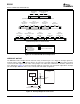
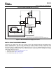
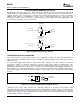
Figure 17 illustrates the SPI port protocol. Byte 0 is referred to as the command byte, where the most significant
bit (or MSB) is the read/write bit. For the R/W bit, a 0 indicates a write operation, while a 1 indicates a read
operation. The remaining seven bits of the command byte are utilized for the register address targeted by the
write or read operation. Byte 1 is a don’t care byte, and may be set to all zeroes. This byte is included in order to
retain protocol compatibility with earlier Texas Instruments digital audio interface and sample rate converter
products, including the DIT4096 , DIT4192 , the SRC418x series devices, and the SRC419x series devices.
21
Submit Documentation Feedback