
DDR2 Memory Controller User's Guide


www.ti.com
DDR2 Memory Controller Registers
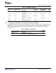
Table 20. SDRAM Configuration Register (SDCFG) Field Descriptions (continued)
Bit Field Value Description
11-9 CL CAS latency. The value of this field defines the CAS latency, to be used when accessing connected
SDRAM devices. A write to this field will cause the DDR2 Memory Controller to start the SDRAM
initialization sequence. This field is writeable only when the TIMUNLOCK bit is unlocked. Values 0,
1, 6, and 7 are reserved for this field.
2 CAS latency of 2
3 CAS latency of 3
4 CAS latency of 4
5 CAS latency of 5
8-7 Reserved Reserved. The reserved bit location is always read as 0. A value written to this field has no effect.
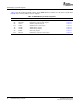
6-4 IBANK Internal SDRAM bank setup bits. Defines number of banks inside connected SDRAM devices. A
write to this bit will cause the DDR2 Memory Controller to start the SDRAM initialization sequence.
Values 4-7 are reserved for this field.
0 One bank SDRAM devices
1 Two banks SDRAM devices
2 Four banks SDRAM devices
3 Eight banks SDRAM devices
3 Reserved Reserved. The reserved bit location is always read as 0. A value written to this field has no effect.
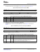
2-0 PAGESIZE Page size bits. Defines the internal page size of the external DDR2 memory. A write to this bit will
cause the DDR2 Memory Controller to start the SDRAM initialization sequence. Values 0, 1, 6, and
7 are reserved for this field. Values 4-7 are reserved for this field.
0 256-word page requiring 8 column address bits.
1 512-word page requiring 9 column address bits.
2 1024-word page requiring 10 column address bits.
3 2048-word page requiring 11 column address bits.
SPRUEK5A – October 2007 DSP DDR2 Memory Controller 39
Submit Documentation Feedback