
Owner's manual

3.1 ADCTL
Registers
www.ti.com
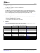
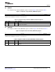
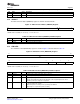
The ADC control register (ADCTL) is shown in Figure 2 and described in Table 2 .
Figure 2. ADC Control (ADCTL) Register
31 24
Reserved
R-0
23 16
Reserved
R-0
15 8
Reserved
R-0
7 6 5 4 3 2 1 0
BUSY CMPFLG CMPIEN CMPMD SCNFLG SCNIEN SCNMD START
R-0 R/C-0 R/W-0 R/W-0 R/C-0 R/W-0 R/W-0 R/W-0
LEGEND: R/W = Read/Write; R = Read only; - n = value after reset
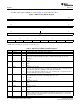
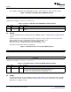
Table 2. ADC Control (ADCTL) Field Descriptions
Bit Field Value Description
31-8 Reserved Any writes to these bit(s) must always have a value of 0.
7 BUSY Busy flag
6 CMPFLG Comparator interrupt flag clear bit. Writing ‘1’ into this bit clears the comparator interrupt flag and
then it will be cleared automatically. At read time, comparator interrupt status can be read.
0 No interrupt
1 Interrupt
5 CMPIEN Comparator interrupt enable bit
0 Disable
1 Enable
4 CMPMD Comparator mode select bit
0 If the value of A/D input data is larger or smaller than the comparative data, a comparator interrupt
is generated. ADC input data < CMPLDAT or ADC input data > CMPUDAT
1 If the value of A/D input data is within the range of the comparative data, a comparator interrupt is
generated. CMPLDAT ≤ ADC input data ≤ CMPUDAT
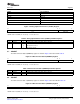
3 SCNFLG Scan interrupt flag clear bit. Writing '1' into this bit clears the scan interrupt flag then it will be
cleared automatically. At read time, scan interrupt status can be read.
0 No interrupt
1 Interrupt
2 SCNIEN Scan interrupt enable bit
0 Disable
1 Enable
1 SCNMD Scan mode selection
0 One shot
1 Free run
0 START A/D conversion start bit The status is cleared automatically when A/D conversion in One-Shot mode
terminates. Writing '0' into this bit in Free-Run mode terminates A/D conversion.'0' can be read at
the time of read-access if no analog channel is selected on the CHSEL register. ('1' can be read
only at the time of A/D conversion.)
Analog to Digital Converter (ADC) Interface12 SPRUFI7 – March 2009
Submit Documentation Feedback