DP83815 DP83815 10/100 Mb/s Integrated PCI Ethernet Media Access Controller and Physical Layer (MacPhyter) Literature Number: SNLS059E
DP83815 10/100 Mb/s Integrated PCI Ethernet Media Access Controller and Physical Layer (MacPhyter™) DP83815 is a single-chip 10/100 Mb/s Ethernet Controller for the PCI bus. It is targeted at low-cost, high volume PC mother boards, adapter cards, and embedded systems. The DP83815 fully implements the V2.2 33 MHz PCI bus interface for host communications with power management support. Packet descriptors and data are transferred via bus-mastering, reducing the burden on the host CPU.
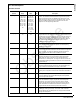
.12.2 MII Serial Management . . . . . . . . . . . . . . . . . . . . 29 1.0 Connection Diagram . . . . . . . . . . . . . . . . . . 4 3.12.3 MII Serial Management Access . . . . . . . . . . . . . 30 1.1 144 LQFP Package (VNG) . . . . . . . . . . . . 4 3.12.4 Serial Management Access Protocol . . . . . . . . . 30 1.2 160 pin LBGA Package (UJB) . . . . . . . . . . 5 3.12.5 Nibble-wide MII Data Interface . . . . . . . . . . . . . . 30 2.0 Pin Description . . . . . . . . . . . . . . . . . . . . . . 6 3.12.
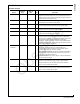
5.2 6.6 Sleep Mode . . . . . . . . . . . . . . . . . . . . . . . 91 6.6.1 Entering Sleep Mode . . . . . . . . . . . . . . . . . . . . . . 91 6.6.2 Exiting Sleep Mode . . . . . . . . . . . . . . . . . . . . . . . . 91 Transmit Architecture . . . . . . . . . . . . . . . 83 6.7 Pin Configuration for Power Management 91 7.0 DC and AC Specifications . . . . . . . . . . . . . 92 5.3 Receive Architecture . . . . . . . . . . . . . . . . 86 7.1 DC Specifications . . . . . . . . . . . . . . . . . . . 92 5.3.
DP83815 1.0 Connection Diagram 36 35 34 33 32 31 30 29 28 27 26 25 24 23 22 21 20 19 18 17 16 15 14 13 12 11 10 9 8 7 6 5 4 3 2 1 FXVDD FXVSS NC PHYVDD2 PHYVSS2 TXCLK TXEN CRS COL/MA16 VDDIO3 VSSIO3 TXD3/MA15 TXD2/MA14 TXD1/MA13 TXD0/MA12 PHYVDD1 PHYVSS1 VDDIO2 X2 X1 VSSIO2 RXDV/MA11 RXER/MA10 RXOE RXD3/MA9 RXD2/MA8 RXD1/MA7 VDDIO1 VSSIO1 RXD0/MA6 RXCLK MDC MDIO MA5 MA4/EECLK MA3/EEDI 1.
DP83815 1.0 Connection Diagram (Continued) 14 13 12 11 10 9 8 7 6 5 4 3 1 Pin A1 Identification (Marked on Top) 2 1.2 160 pin LBGA Package (UJB) A B te C D E G H J K L M bs N ol e F O P Top View Order Number DP83815DUJB See NS Package Number UJB160A 5 www.national.
DP83815 2.0 Pin Description PCI Bus Interface CBEN[3-0] LBGA Pin No(s) 66, 67, 68, 70, 71, 72, 73, 74, 78, 79, 81, 82, 83, 86, 87, 88, 101, 102, 104, 105, 106, 108, 109, 110, 112, 113, 115, 116, 118, 119, 120, 121 K3, K2, K4, L3, L2, M1, N3, P3, L4 N5, M5, L5, N6, L6, N7, P7, N10, L10, M11, N11, P12, N12, M13, M14, L12, L14, K13, K14, K11, J13, J14, J12 I/O Address and Data: Multiplexed address and data bus. As a bus master, the DP83815 will drive address during the first bus phase.
DP83815 2.0 Pin Description (Continued) PCI Bus Interface LBGA Pin No(s) Dir Description PERRN 97 N9 I/O Parity Error: The DP83815 as a master or target will assert this signal low to indicate a parity error on any incoming data (except for special cycles). As a bus master, it will monitor this signal on all write operations (except for special cycles). REQN 64 J4 O Request: The DP83815 will assert this signal low to request ownership of the bus from the central arbiter.
DP83815 2.0 Pin Description (Continued) Media Independent Interface (MII) LQFP Pin No(s) LBGA Pin No(s) Dir COL 28 C5 I Collision Detect: The COL signal is asserted high asynchronously by the external PMD upon detection of a collision on the medium. It will remain asserted as long as the collision condition persists. CRS 29 B5 I Carrier Sense: This signal is asserted high asynchronously by the external PMD upon detection of a non-idle medium.
DP83815 2.0 Pin Description (Continued) 100BASE-TX/10BASE-T Interface Symbol LQFP Pin No(s) LBGA Pin No(s) Dir Description TPTDP, TPTDM 54, 53 G1, F1 A-O Transmit Data: Differential common output driver. This differential common output is configurable to either 10BASE-T or 100BASE-TX signaling: 10BASE-T: Transmission of Manchester encoded 10BASE-T packet data as well as Link Pulses (including Fast Link Pulses for AutoNegotiation purposes).
DP83815 2.0 Pin Description (Continued) Clock Interface LBGA Pin No(s) Dir Description X1 17 D8 I Crystal/Oscillator Input: This pin is the primary clock reference input for the DP83815 and must be connected to a 25 MHz 0.005% (50ppm) clock source. The DP83815 device supports either an external crystal resonator connected across pins X1 and X2, or an external CMOS-level oscillator source connected to pin X1 only.
DP83815 2.0 Pin Description (Continued) External Reference Interface Symbol VREF LQFP Pin No(s) LBGA Pin No(s) Dir Description 40 A2 I Bandgap Reference: External current reference resistor for internal Phy bandgap circuitry. The value of this resistor is 9.31 KΩ 1% metal film (100 ppm/oC) which must be connected from the VREF pin to analog ground.
DP83815 2.0 Pin Description (Continued) Supply Pins LQFP Pin No(s) LBGA Pin No(s) Dir SUBGND1, SUBGND2, SUBGND3 37, 49, 126 B2, E1, G12 S Substrate GND RXAVDD1, RXAVDD2 39, 47 C2, E2 S RX Analog VDD - connect to isolated Aux 3.3V supply VDD RXAVSS1, RXAVSS2 38, 44 B1, D3 S RX Analog GND TXIOVSS1, TXIOVSS2 52, 55 F2, G4 S TX Output driver VSS TXDVDD 56 H3 S TX Digital VDD - connect to Aux 3.
DP83815 consists of a MAC/BIU (Media Access Controller/Bus Interface Unit), a physical layer interface, SRAM, and miscellaneous support logic. The MAC/BIU includes the PCI bus, BIOS ROM and EEPROM interfaces, TPRDP/M and an 802.3 MAC. The physical layer interface used is a single-port version of the 3.3V DsPhyter. Internal memory consists of one - 0.5 KB and two - 2 KB SRAM blocks. Test data in Interface Logic ol e SRAM RXFilter .
DP83815 3.0 Functional Description (Continued) 32 15 32 Data FIFO 4 32 Tx Buffer Manager 32 32 PCI Bus Interface 32 Data FIFO 4 Rx MAC te PCI Bus 32 Rx Buffer Manager MIB ol e 32 32 Rx Filter Pkt Recog Logic 16 SRAM Physical Layer Interface Tx MAC bs MAC/BIU O 93C46 Serial EEPROM Boot ROM/ Flash Figure 3-2 MAC/BIU Functional Block Diagram 3.1 MAC/BIU The MAC/BIU is a derivative design from the DP83810 (Euphrates).
3.2 Buffer Management Little Endian (CFG:BEM=0): The byte orientation for receive and transmit data in system memory is as follows: 31 24 23 16 15 8 7 The buffer management scheme used on the DP83815 allows quick, simple and efficient use of the frame buffer memory. Frames are saved in similar formats for both transmit and receive. The buffer management scheme also uses separate buffers and descriptors for packet information.
3.3.2 Boot PROM The standard 802.3 Ethernet packet consists of the following fields: Preamble (PA), Start of Frame Delimiter (SFD), Destination Address (DA), Source Address (SA), Length (LEN), Data and Frame Check Sequence (FCS). All fields are fixed length except for the data field. During reception, the PA, SFD and FCS are stripped. During transmission, the DP83815 generates and appends the PA, SFD and FCS.
DP83815 3.
3.4 Physical Layer operation when the Auto-Negotiation Enable bit (bit 12) is set. The DP83815 has a full featured physical layer device with integrated PMD sub-layers to support both 10BASE-T and 100BASE-TX Ethernet protocols. The physical layer is designed for easy implementation of 10/100 Mb/s Ethernet home or office solutions. It interfaces directly to twisted pair media via an external transformer.
The LED100N pin indicates a good link at 100 Mb/s data rate. The standard CMOS driver goes low when this occurs. In 100BASE-T mode, link is established as a result of input receive amplitude compliant with TP-PMD specifications which will result in internal generation of signal detect. This signal will assert after the internal Signal Detect has remained asserted for a minimum of 500 us. The signal will de-assert immediately following the deassertion of the internal signal detect. register is set to a one.
3.6 Half Duplex vs. Full Duplex In 100BASE-TX Loopback mode the data is routed through the PCS and PMA layers into the PMD sublayer before it is The DP83815 supports both half and full duplex operation looped back. Therefore, in addition to serving as a board at both 10 Mb/s and 100 Mb/s speeds. diagnostic, this mode serves as quick functional verification Half-duplex is the standard, traditional mode of operation of the device.
DP83815 3.0 Functional Description (Continued) TXCLK TXD(3:0)/TXER FROM CGM 4B5B CODEGROUP ENABLER MUX BP_4B5B te 5B PARALLEL TO SERIAL SCRAMBLER MUX ol e BP_SCR MUX NRZ TO NRZI ENCODER O bs 100BASE-TX LOOPBACK BINARY TO MLT-3/ COMMON DRIVER TD +/- Figure 3-6 100BASE-TX Transmit Block Diagram 3.9.1 Code-group Encoding and Injection 3.9.2 Scrambler The code-group encoder converts 4-bit (4B) nibble data generated by the MAC into 5-bit (5B) code-groups for transmission.
3.9.3 NRZ to NRZI Encoder 3.9.4 Binary to MLT-3 Convertor / Common Driver After the transmit data stream has been serialized and scrambled, the data must be NRZI encoded in order to comply with the TP-PMD standard for 100BASE-TX transmission over Category-5 un-shielded twisted pair cable. There is no ability to bypass this block within the DP83815.
DP83815 3.0 Functional Description (Continued) Table 3-1 4B5B Code-Group Encoding/Decoding PCS 5B Code-group Description/4B Value 00000 00001 00010 00011 00101 00110 01000 01100 10000 11001 The 100BASE-TX MLT-3 signal sourced by the TD± common driver output pins is slew rate controlled. This should be considered when selecting AC coupling magnetics to ensure TP-PMD Standard compliant transition times (3 ns < Tr < 5 ns). 3.10.
SD RXD(3:0)/RXER RXCLK BP_RX MUX MUX BP_4B5B 4B/5B DECODER LINK INTEGRITY MONITOR te SERIAL TO PARALLEL RX_DATA VALID CODE GROUP ALIGNMENT ol e SSD DETECT MUX BP_SCR DESCRAMBLER CLOCK CLOCK NRZI TO NRZ DECODER bs RECOVERY MODULE O MLT-3 TO BINARY DECODER DIGITAL ADAPTIVE EQUALIZATION AGC SIGNAL DETECT INPUT BLW COMPENSATION ADC RD +/- Figure 3-8 100 M/bs Receive Block Diagram Subject to change without notice. 24 Rev O www.national.com DP83815 3.
DP83815 ol e te 3.0 Functional Description (Continued) Figure 3-9 100BASE-TX BLW Event Diagram it is sensitive to transformer mismatch, resistor variation and process induced offset. The DP83223V also required When transmitting data at high speeds over copper twisted an external attenuation network to help match the incoming pair cable, frequency dependent attenuation becomes a signal amplitude to the internal reference. concern.
DP83815 te 3.0 Functional Description (Continued) 2ns/div ol e Figure 3-12 MLT-3 Signal Measured at AII after 50 meters of CAT V cable O bs Figure 3-10 EIA/TIA Attenuation vs. Frequency for 0, 50, 100, 130 & 150 meters of CAT V cable 2ns/div 2ns/div Figure 3-11 MLT-3 Signal Measured at AII after 0 meters of CAT V cable Figure 3-13 MLT-3 Signal Measured at AII after 100 meters of CAT V cable 3.10.
recognize sufficient unscrambled IDLE code-groups within the 722 µs period, the entire de-scrambler will be forced out of the current state of synchronization and reset in order to re-acquire synchronization. 3.10.6 Clock Recovery Module The Clock Recovery Module (CRM) accepts 125 Mb/s MLT3 data from the equalizer. The DPLL locks onto the 125 Mb/s data stream and extracts a 125 MHz recovered clock.
3.11 10BASE-T Transceiver Module The squelch circuitry employs a combination of amplitude and timing measurements (as specified in the IEEE 802.3 The 10BASE-T Transceiver Module is IEEE 802.3 10BASE-T standard) to determine the validity of data on compliant. It includes the receiver, transmitter, collision, the twisted pair inputs (refer to Figure 3-14). heartbeat, loopback, jabber, and link integrity functions, as defined in the standard.
clock signals and data. The differential input must be externally terminated with a differential 100Ω termination network to accommodate UTP cable. The internal impedance of RD± (typically 1.1Kohms) is in parallel with two 54.9 resistors to approximate the 100Ω termination. 3.11.5 Jabber Function The jabber function monitors the DP83815's output and disables the transmitter if it attempts to transmit a packet of longer than legal size.
3.12.3 MII Serial Management Access 3.12.4 Serial Management Access Protocol Management access to the PHY(s) is done via Management Data Clock (MDC) and Management Data Input/Output (MDIO). MDC has a maximum clock rate of 25 MHz and no minimum rate. The MDIO line is bi-directional and may be shared by up to 32 devices. The internal PHY counts as one of these 32 devices. The serial control interface clock (MDC) has a maximum clock rate of 25 MHz and no minimum rate.
DP83815 3.0 Functional Description (Continued) MDC MDIO Z Z (STA) Z Idle 0 1 0 1 0 1 1 0 0 0 0 0 0 0 1 0 0 0 0 0 0 0 0 0 0 0 0 0 0 0 0 0 Start Opcode (Write) PHY Address (PHYAD = 0Ch) Register Address (00h = BMCR) TA Z Idle Register Data Figure 3-16 Typical MDC/MDIO Write Operation The transmit interface consists of a nibble wide data bus TXD[3:0], a transmit enable control signal TXEN, and a transmit clock TXCLK which runs at 2.5 MHz or 25 MHz.
4.1 Configuration Registers The DP83815 implements a PCI version 2.2 configuration register space. This allows a PCI BIOS to "soft" configure the DP83815. Software Reset has no effect on configuration registers. Hardware Reset returns all configuration registers to their hardware reset state. For all unused registers, writes are ignored, and reads return 0.
4.1.2 Configuration Command and Status Register The CFGCS register has two parts. The upper 16-bits (31-16) are devoted to device status. A status bit is reset whenever the register is written, and the corresponding bit location is a 1. The lower 16-bits (15-0) are devoted to command and are used to configure and control the device.
DP83815 4.0 Register Set (Continued) Bit Bit Name 6 PERRSP Description Parity Error Response When set, DP83815 will assert PERRN on the detection of a data parity error when acting as the target, and will sample PERRN when acting as the initiator. Also, setting PERRSP allows SERREN to enable the assertion of SERRN. When reset, all address and data parity errors are ignored and neither SERRN nor PERRN are asserted.
4.1.4 Configuration Latency Timer Register This register gives status and controls such miscellaneous functions as BIST, Latency timer and Cache line size. Tag: CFGLAT Offset: 0Ch Bit Bit Name 31 BISTCAP Size: 32 bits Access: Read Write Hard Reset: 00000000h Soft Reset: Unchanged Description BIST Capable Reads will always return 0. 30 BISTEN BIST Enable Reads will return a 0, writes are ignored. 29-16 Reserved 15-8 LAT Latency Timer te Reads will return a 0, writes are ignored.
4.1.6 Configuration Memory Address Register This register specifies the Base Memory address which is required to build an address map during configuration. It also specifies the number of bytes required as well as an indication that it can be mapped into memory space.
DP83815 4.0 Register Set (Continued) 4.1.8 Boot ROM Configuration Register Tag: CFGROM Offset: 30h Bit Bit Name 31-16 ROMBASE 15-11 ROMSIZE Size: 32 bits Access: Read Write Hard Reset: 00000000h Soft Reset: unchanged Description ROM Base Address Set to the base address for the boot ROM. ROM Size Set to 0 indicating a requirement for 64K bytes of Boot ROM space. Read only. 10-1 unused (reads return 0) ROMEN ROM Enable te 0 ol e This is used by the PCI BIOS to enable accesses to boot ROM.
4.1.10 Configuration Interrupt Select Register This register stores the interrupt line number as identified by the POST software that is connected to the interrupt controller as well as DP83815 desired settings for maximum latency and minimum grant. Max latency and Min latency can be loaded from the EEPROM.
DP83815 4.0 Register Set (Continued) Bit Bit Name 24-22 Description AUX_CURRENT Aux_Current This 3 bit field reports the 3.3Vaux auxiliary current requirements for the PCI function. If PMEN generation from D3cold is not supported by the function(PMCAP[31]), this field returns a value of "000b" when read. 21 DSI Bit 3.3Vaux 24 23 22 Max.
4.2 Operational Registers The DP83815 provides the following set of operational registers mapped into PCI memory space or I/O space. Writes to reserved register locations are ignored. Reads to reserved register locations return undefined values.
4.2.1 Command Register This register is used for issuing commands to DP83815. These commands are issued by setting the corresponding bits for the function. A global software reset along with individual reset and enable/disable for transmitter and receiver are provided here.
4.2.2 Configuration and Media Status Register This register allows configuration of a variety of device and phy options, and provides phy status information. Tag: CFG Size: 32 bits Offset: 0004h Bit Bit Name 31 LNKSTS Access: Read Write Hard Reset: 00000000h Soft Reset: 00000000h Description Link Status Link status of the internal phy. Asserted when link is good. RO 30 SPEED100 Speed 100 Mb/s Speed 100 Mb/s indicator for internal phy. Asserted when speed is set or has negotiated to 100 Mb/s.
DP83815 4.0 Register Set (Continued) Bit Bit Name 10 PHY_RST Description Reset internal Phy Asserts reset to internal phy. Can be used to cause phy to reload options from the CFG register. This bit does not self clear when set. R/W 9 PHY_DIS Disable internal Phy When set to a 1, this bit forces the internal phy to its low-power state. R/W 8 EUPHCOMP DP83810 Descriptor Compatibility When set, DP83815 will use DP83810 compatible (but single fragment) descriptor format.
4.2.3 EEPROM Access Register The EEPROM Access Register provides an interface for software access to the NMC9306 style EEPROM The default values given assume that the EEDO line has a pullup resistor to VDD. Tag: MEAR Size: 32 bits Offset: 0008h Bit 6 Access: Read Write Bit Name 31-7 Hard Reset: 00000002h Soft Reset: 00000002h Description unused MDC MII Management Clock Controls the value of the MDC pin. When set, the MDC pin is 1; when clear the MDC pin is 0.
PMATCH[47:0] can be accessed via the combination of the RFCR (offset 0048h) and RFDR (offset 004Ch) registers. PMATCH holds the Ethernet address info. See Section 3.3.3. The lower 8 bits of the checksum value should be 55h. For the upper 8 bits, add the top 8 data bits to the lower 8 data bits for each address. Sum the resultant 8 bit values for all addresses and then add 55h. Take the 2’s complement of the final sum.
4.2.6 Interrupt Status Register This register indicates the source of an interrupt when the INTA pin goes active. Enabling the corresponding bits in the Interrupt Mask Register (IMR) allows bits in this register to produce an interrupt. When an interrupt is active, one or more bits in this register are set to a “1”. The Interrupt Status Register reflects all current pending interrupts, regardless of the state of the corresponding mask bit in the IMR. Reading the ISR clears all interrupts.
DP83815 4.0 Register Set (Continued) Bit Bit Name 7 TXDESC Description Tx Descriptor This event is signaled after a transmit descriptor when the INTR bit in the CMDSTS field has been updated. 6 TXOK Tx Packet OK This event is signaled after the last transmit descriptor in a successful transmission attempt has been updated with valid status. 5 RXORN 4 RXIDLE Rx Overrun Set when a receive data FIFO overrun condition occurs.
DP83815 4.0 Register Set (Continued) Bit Bit Name 20 RTABT Description Received Target Abort When this bit is 0, the corresponding bit in the ISR will not cause an interrupt. 19-17 16 unused RXSOVR Rx Status FIFO Overrun When this bit is 0, the corresponding bit in the ISR will not cause an interrupt. 15 HIERR High Bits Error When this bit is 0, the corresponding bit in the ISR will not cause an interrupt.
DP83815 4.0 Register Set (Continued) 4.2.8 Interrupt Enable Register The Interrupt Enable Register controls the hardware INTR signal. Tag: IER Offset: 0018h Bit Access: Read Write Bit Name 31-1 0 Size: 32 bits Hard Reset: 00000000h Soft Reset: 00000000h Description unused IE Interrupt Enable 4.2.9 Transmit Descriptor Pointer Register This register points to the current Transmit Descriptor.
4.2.10 Transmit Configuration Register This register defines the Transmit Configuration for DP83815. It controls such functions as Loopback, Heartbeat, Auto Transmit Padding, programmable Interframe Gap, Fill & Drain Thresholds, and maximum DMA burst size.
DP83815 4.
4.2.12 Receive Configuration Register This register is used to set the receive configuration for DP83815. Receive properties such as accepting error packets, runt packets, setting the receive drain threshold etc. are controlled here. Tag: RXCFG Offset: 0034h Bit Bit Name 31 AEP Size: 32 bits Access: Read Write Hard Reset: 00000002h Soft Reset: 00000002h Description Accept Errored Packets When set to 1, all packets with CRC, alignment, and/or collision errors will be accepted.
DP83815 4.0 Register Set (Continued) Bit Bit Name 5-1 DRTH Description Rx Drain Threshold Specifies the drain threshold in units of 8 bytes. When the number of bytes in the receive FIFO reaches this value (times 8), or the FIFO contains a complete packet, the receive bus master state machine will begin the transfer of data from the FIFO to host memory. Care must be taken when setting DRTH to a value lower than the number of bytes needed to determine if packet should be accepted or rejected.
Situation 1 is a “clock continue” event and can occur if the DP83815 has not completed a pending packet transmit or receive. Situation 2 is a “clock start” event and can occur if the DP83815 has been programmed to a WOL state and it receives a wake packet, or the PCI clock has simply been stopped and the receiver has data ready to DMA.
4.2.14 Wake Command/Status Register The WCSR register is used to configure/control and monitor the DP83815 Wake On LAN logic. The Wake On LAN logic is used to monitor the incoming packet stream while in a low-power state, and provide a wake event to the system if the desired packet type, contents, or Link change are detected.
DP83815 4.0 Register Set (Continued) Bit Bit Name 5 WKPAT0 4 WKARP 3 WKBCP 2 WKMCP 1 WKUCP 0 WKPHY Description Wake on Pattern 0 match Enable wake on match of pattern 0. R/W Wake on ARP Enable wake on ARP packet detection. R/W Wake on Broadcast Enable wake on broadcast packet detection. R/W Wake on Multicast Enable wake on multicast packet detection. R/W Wake on Unicast Enable wake on unicast packet detection. R/W Wake on Phy Interrupt 4.2.14.1 Wake on LAN host memory for processing.
4.2.15 Pause Control/Status Register The PCR register is used to control and monitor the DP83815 Pause Frame reception logic. The Pause Frame reception Logic is used to accept 802.3x Pause Frames, extract the pause length value, and initiate a TX MAC pause interval of the specified number of slot times. Tag: PCR Offset: 0044h Bit Bit Name 31 PSEN Size: 32 bits Access: Read Write Hard Reset: 00000000h Soft Reset: 00000000h Description Pause Enable Manually enables reception of 802.
4.2.16 Receive Filter/Match Control Register The RFCR register is used to control and configure the DP83815 Receive Filter Control logic. The Receive Filter Control Logic is used to configure destination address filtering of incoming packets. Tag: RFCR Offset: 0048h Bit Bit Name 31 RFEN Size: 32 bits Access: Read Write Hard Reset: 00000000h Soft Reset: 00000000h Description Rx Filter Enable When this bit is set to 1, the Rx Filter is enabled to qualify incoming packets.
DP83815 4.
DP83815 4.0 Register Set (Continued) 4.2.18 Receive Filter Logic Accept on Pattern Match The Receive Filter Logic supports a variety of techniques for qualifying incoming packets. The most basic filtering options include Accept All Broadcast, Accept All Multicast and Accept All Unicast packets. These options are enabled by setting the corresponding bit in the Receive Filter Control Register, RFCR.
DP83815 Mask Bit Byte0 Mask Bit Byte1 4.0 Register Set (Continued) 3FE Pattern2Word7F byte1 byte0 3FC Pattern3Word7E byte1 byte0 3FA Pattern2Word7E byte1 byte0 3F8 .................... byte1 byte0 306 te Pattern3Word1 .................... byte0 .................... byte1 ....................
DP83815 4.
Accept on Multicast or Unicast Hash Hash Table memory. The upper 4 bits represent the word address and the lower 5 bits select the bit within the word. If the corresponding bit is set, then the packet is accepted, otherwise the packet is rejected. The hash table memory is accessed through the RFCR and the RFDR. Refer to Figure 4-2 for a memory map. Below is example code for setting/clearing a bit in the hash table.
DP83815 4.0 Register Set (Continued) 4.2.19 Boot ROM Address Register The BRAR is used to setup the address for an access to an external ROM/FLASH device. Tag: BRAR Offset: 0050h Bit Bit Name 31 AUTOINC Size: 32 bits Access: Read Write Hard Reset: FFFFFFFFh Soft Reset: unchanged Description Auto-Increment When set, the contents of ADDR will auto increment with every 32-bit access to the BRDR register.
4.2.22 Management Information Base Control Register The MIBC register is used to control access to the statistics block and the warning bits and to control the collection of management information statistics.
4.2.23 Management Information Base Registers "software" counters must be updated. Sizes for specific hardware statistic counters were chosen such that the count values will not roll over in less than 15 ms if incremented at the theoretical maximum rates described in the above specifications. However, given that the theoretical maximum counter rates do not represent realistic network traffic and events, the actual rollover rates for the hardware counters are more likely to be on the order of several seconds.
4.3 Internal PHY Registers The Internal Phy Registers are only 16 bits wide. Bits [31:16] are not used.
Bit 7 6:0 Bit Name Description Collision Test Collision Test: Default: 0 1 = Collision test enabled 0 = Normal operation When set, this bit will cause the COL signal to be asserted in response to the assertion of TXEN within 512-bit times. The COL signal will be de-asserted within 4-bit times in response to the de-assertion of TXEN. Reserved Reserved: Default: 0, RO 4.3.
4.3.3 PHY Identifier Register #1 The PHY Identifier Registers #1 and #2 together form a unique identifier for the PHY section of this device. The Identifier consists of a concatenation of the Organizationally Unique Identifier (OUI), the vendor's model number and the model revision number. A PHY may return a value of zero in each of the 32 bits of the PHY Identifier if desired. The PHY Identifier is intended to support network management. National Semiconductor's IEEE assigned OUI is 080017h.
DP83815 4.
DP83815 4.0 Register Set (Continued) Bit Bit Name 5 10 10BASE-T Support: 1 = 10BASE-T is supported by the Link Partner 0 = 10BASE-T not supported by the Link Partner Description 4:0 Selector Protocol Selection Bits: Link Partners’s binary encoded protocol selector. 4.3.7 Auto-Negotiate Expansion Register This register contains additional Local Device and Link Partner status information.
Bit Bit Name 12 ACK2 Acknowledge2: Default: 0 1 = Will comply with message 0 = Cannot comply with message Acknowledge2 is used by the next page function to indicate that Local Device has the ability to comply with the message received.
Bit Bit Name Description 6 Remote Fault Remote Fault: 1 = Remote Fault condition detected (cleared on read of BMSR (address 0x84h) register or by reset). Fault criteria: notification from Link Partner of Remote Fault via Auto-Negotiation 0 = No remote fault condition detected 5 Jabber Detect Jabber Detect: This bit only has meaning in 10 Mb/s mode This bit is a duplicate of the Jabber Detect bit in the BMSR register, except that it is not cleared upon a read of the PHYSTS register.
4.3.10 MII Interrupt Control Register This register implements the MII Interrupt PHY Specific Control register. Sources for interrupt generation include: Link State Change, Jabber Event, Remote Fault, Auto-Negotiation Complete or any of the counters becoming half-full. Note that the TINT bit operates independently of the INTEN bit. In other words, INTEN does not need to be active to generate the test interrupt.
4.3.12 False Carrier Sense Counter Register This counter provides information required to implement the “FalseCarriers” attribute within the MAU managed object class of Clause 30 of the IEEE 802.3u specification. Tag: FCSCR Offset: 00D0h Bit Size: 16 bits Access: Read Write Bit Name 15:8 Description Reserved Reserved: Writes ignored, Read as 0 FCSCNT[7:0] False Carrier Event Counter: Default: 0, RW/COR This 8-bit counter increments on every false carrier event.
DP83815 4.0 Register Set (Continued) Bit Bit Name 8 SD_OPTION 7:6 Reserved Reserved: Read as 0 FORCE_100_OK Force 100 Mb/s Good Link: OR’ed with MAC_FORCE_LINK_100 signal. 1 = Forces 100 Mb/s Good Link 0 = Normal 100 Mb/s operation 4:3 Reserved Reserved: Read as 0 2 NRZI_BYPASS 1:0 Reserved NRZI Bypass Enable: 1 = NRZI Bypass Enabled 0 = NRZI Bypass Disabled Reserved: Read as 0 4.3.
DP83815 4.0 Register Set (Continued) 4.3.16 10BASE-T Status/Control Register Tag: TBTSCR Offset: 00E8h Bit 15:9 8 Size: 16 bits Hard Reset: 0004h Access: Read Write Bit Name Description Unused LOOPBACK_10_DIS 10BASE-T Loopback Disable: This bit is OR’ed with bit 14 (Loopback) in the BMCR. 1 = 10 Mb/s Loopback is enabled 0 = 10 Mb/s Loopback is disabled LP_DIS Normal Link Pulse Disable: This bit is OR’ed with the MAC_FORCE_LINK_10 signal.
DP83815 4.0 Register Set (Continued) 4.4 Recommended Registers Configuration For optimum performance of the DP83815, version noted as DP83815CVNG (SRR = 302h), the listed register modifications must be followed in sequence. The table below contains the register’s offset address value. The register address consists of: I/O Base Address + Offset Address. All values are given in hex. Register Tag Offset Address Register Value 1. 00CCh PGSEL 0001h 2. 00E4h PMDCSR 189Ch 3. 00FCh TSTDAT 0000h 4.
5.1 Overview The buffer management scheme used on the DP83815 allows quick, simple and efficient use of the frame buffer memory. Frames are saved in similar formats for both transmit and receive. The buffer management scheme also uses separate buffers and descriptors for packet information. This allows effective transfers of data from the receive buffer to the transmit buffer by simply transferring the descriptor from the receive queue to the transmit queue.
27 OK 26-16 --- Packet OK The usage of these bits differ in receive and transmit descriptors. See below for details. 15-12 11-0 In the last descriptor in a packet, this bit indicates that the packet was either sent or received successfully. (reserved) SIZE Descriptor Byte Count Set to the size in bytes of the data. Table 5-3 Transmit Status Bit Definitions Tag Description Usage 26 TXA Transmit Abort Transmission of this packet was aborted.
DP83815 5.0 Buffer Management (Continued) Table 5-4 Receive Status Bit Definitions Bit Tag 26 RXA Receive Aborted Description Set to 1 by DP83815 when the receive was aborted, the value of this bit always equals RXO. Exists for backward compatibility. Usage 25 RXO Receive Overrun Set to 1 by DP83815 to indicate that a receive overrun condition occurred. RXA will also be set.
5.1.3 Multiple Descriptor Packets 5.1.4 Descriptor Lists A single packet may also cross descriptor boundaries. This is indicated by setting the MORE bit in all descriptors except the last one in the packet. Ethernet applications (bridges, switches, routers, etc.) can optimize memory utilization by using a single small buffer per receive descriptor, and allowing the DP83815 hardware to use the minimum number of buffers necessary to store an incoming packet.
DP83815 5.0 Buffer Management (Continued) 5.2 Transmit Architecture The following figure illustrates the transmit architecture of the DP83815 10/100 Ethernet Controller. Software/Memory Hardware Current Tx Desc Ptr Transmit Descriptor TxHead link cmdsts ptr Tx Desc Cache link cmdsts ptr Packet te Tx Data FIFO Tx DMA Figure 5-4 Transmit Architecture 5.2.
DP83815 5.0 Buffer Management (Continued) Table 5-5 Transmit State Tables State Event Next State txIdle CR:TXE && !CTDD txDescRead Start a burst transfer at address TXDP and a length derived from TXCFG. CR:TXE && CTDD txDescRefr Start a burst transfer to refresh the link field of the current descriptor. txDescRefr XferDone txAdvance txDescRead XferDone && OWN txFIFOblock XferDone && !OWN txIdle FifoAvail txFragRead txFIFOblock Actions Set ISR:TXIDLE.
5.2.2 Transmit Data Flow O bs ol e 1. The device driver receives packets from an upper layer. 2. An available DP83815 transmit descriptor is allocated. The fragment information is copied from the NOS specific data structure(s) to the DP83815 transmit descriptor. 3. The driver adds this descriptor to it’s internal list of transmit descriptors awaiting transmission. 4.
5.3 Receive Architecture packets. When the amount of receive data in the RxDataFIFO is more than the RxDrainThreshold, or the RxDataFIFO contains a complete packet, then the state machine begins filling received buffers in host memory. The receive architecture is as "symmetrical" to the transmit architecture as possible.
DP83815 5.0 Buffer Management (Continued) Table 5-6 Receive State Tables State Event Next State rxIdle CR:RXE && !CRDD rxDescRead Start a burst transfer at address RXDP and a length derived from RXCFG. CR:RXE && CRDD rxDescRefr Start a burst transfer to refresh the link field of the current descriptor. rxDescRefr XferDone rxAdvance rxDescRead XferDone && !OWN rxFIFOblock XferDone && OWN rxIdle FifoReady rxFragWrite Start a burst transfer from the RxDataFIFO to host memory at fragPtr.
DP83815 5.0 Buffer Management (Continued) CR:RXE && CRDD rxDescRefr CR:RXE && !CRDD XferDone rxIdle XferDone && OWN link = NULL link != NULL rxDescRead te rxAdvance XferDone && !OWN XferDone ol e rxPktBytes == 0 FifoReady rxDescWrite rxFifoBlock (descCnt == 0) && (rxPktBytes > 0) rxFragWrite XferDone Figure 5-7 Receive State Diagram bs 5.3.
6.1 Introduction • Magic Packet: “A specific packet of information sent to remotely wake up a sleeping or powered off PC on a network, it is handled in the LAN controller. The Magic Packet must contain a specific data sequence which can be located anywhere within the packet but must be preceded by a synchronization stream. The packet must also meet the basic requirements for the LAN technology chosen (e.g. ethernet frame).
6.4.1 D0 State 6.5.1 Entering WOL Mode The D0 state is the normal operational state of the device. The PME Enable bit should be set to 0 to prevent packet filtering based on the settings in the Wake Control/Status Register (WCSR). It is also advisable to turn off all WOL conditions in WCSR to prevent unnecessary PME interrupts. The following steps are required to place the DP83815 into WOL mode: 1.
6.5.2 Wake Events 6.6 Sleep Mode If the device detects a wake event while in WOL mode, it will assert the PMEN pin low to signal the system that a wake event has occurred. The system should then bring the device out of WOL mode as described below. Sleep Mode is a system-level function that allows a device to be placed in a lower power mode than WOL mode. In sleep mode, the device will not be able to detect wake events or signal the system that it needs service. 6.5.3 Exiting WOL Mode 6.6.
Absolute Maximum Ratings Supply Voltage (VDD) -0.5 V to 3.6 V 3.3 V PCI signaling, 5.0 V tolerant DC Input Voltage (VIN) -0.5 V to 7.0 V DC Output Voltage (VOUT) For LBGA Package: θja (@0 cfm, 1 Watt) Recommended Operating Conditions Supply voltage (VDD) -0.5 V to VDD + 0.5 V Storage Temperature Range (TSTG) 220 °C ESD Rating 2.0 KV te 9.5 °C/W 7.1 DC Specifications o o TA = 0 C to 70 C, VDD = 3.3 V ±0.
DP83815 7.0 DC and AC Specifications (Continued) 7.2 AC Specifications 7.2.1 PCI Clock Timing T3 T1 PCICLK Parameter PCICLK Low Time 7.2.1.2 PCICLK High Time 7.2.1.3 PCICLK Cycle Time 7.2.2 X1 Clock Timing Max Units 12 ns 12 ns 30 ∞ ns ol e 7.2.1.1 Min te Number T2 T3 T1 T2 bs X1 Number Parameter Min Max Units X1 Low Time 16 ns 7.2.2.2 X1 High Time 16 ns O 7.2.2.1 7.2.2.3 X1 Cycle Time 40 93 40 ns www.national.
DP83815 7.0 DC and AC Specifications (Continued) 7.2.3 Power On Reset (PCI Active) Power Stable T1 RSTN T2 1st PCI Cycle PCICLK Number Parameter te Reset Complete Min RSTN Active Duration from PCICLK stable 7.2.3.2 Reset Disable to 1st PCI Cycle 1 Units ms ol e 7.2.3.1 Max EE Enabled 1500 us EE Disabled 1 us Note 1: Minimum reset complete time is a function of the PCI, transmit, and receive clock frequencies. Note 2: Minimum access after reset is dependent on PCI clock frequency.
DP83815 7.0 DC and AC Specifications (Continued) 7.2.5 POR PCI Inactive VDD T1 EESEL T2 TPRD 7.2.5.1 Parameter VDD stable to EE access Min Max Units te Number T3 60 us 2000 us VDD indicates the digital supply (AUX power plane, except PCI bus power.) Guaranteed by design. EE Configuration load duration 7.2.5.3 EE Cfg. load complete to RX ready: ol e 7.2.5.2 600 - Auto-Neg or 10 Mb TBD us O bs - 100 Mb 95 www.national.
DP83815 7.0 DC and AC Specifications (Continued) 7.2.6 PCI Bus Cycles The following table parameters apply to ALL the PCI Bus Cycle Timing Diagrams contained in this section. Number Parameter Min Max Units 7.2.6.1 Input Setup Time 7 ns 7.2.6.2 Input Hold Time 0 ns 7.2.6.3 Output Valid Delay 2 7.2.6.4 Output Float Delay (toff time) 7.2.6.5 Output Valid Delay for REQN - point to point 2 7.2.6.
DP83815 7.0 DC and AC Specifications (Continued) PCI Configuration Write PCICLK FRAMEN AD[31:0] T1 T1 T1 C/BEN[3:0] T1 T2 T2 T2 T1 Addr Data T2 T1 Cmd T2 T2 BE IDSEL T2 T4 te T1 IRDYN T3 TRDYN T4 T3 DEVSELN T1 T2 T2 ol e PAR T4 T3 PERRN PCI Bus Master Read T4 bs PCICLK FRAMEN T3 C/BEN[3:0] T3 Cmd O AD[31:0] T3 Addr IRDYN T3 T4 T1 T3 T1 T2 Data T4 BE T3 T3 T4 T2 T1 TRDYN T1 T2 DEVSELN T4 T3 T2 T1 PAR T3 PERRN 97 T3 T4 www.national.
DP83815 7.0 DC and AC Specifications (Continued) PCI Bus Master Write PCICLK T3 T3 T3 Data T4 AD[31:0] T3 Addr T3 Cmd T3 T4 C/BEN[3:0] FRAMEN T4 BE T3 T3 IRDYN T2 T1 DEVSELN T3 T3 T2 T4 ol e PAR te T1 TRDYN T4 T1 PERRN PCI Target Read bs PCICLK FRAMEN T1 Addr T1 T2 IRDYN TRDYN DEVSELN T2 T4 T4 T3 T3 Data T1 Cmd O C/BEN[3:0] T4 T2 T1 T2 AD[31:0] T2 T2 BE T2 T1 T3 T3 T1 T2 T4 T4 T3 T3 PAR T1 T4 T1 PERRN 98 www.national.
DP83815 7.0 DC and AC Specifications (Continued) PCI Target Write PCICLK FRAMEN AD[31:0] T1 T2 T1 T2 Addr T1 C/BEN[3:0] T2 T1 Data T2 T1 Cmd BE T2 T1 IRDYN T4 te T3 TRDYN T4 T3 DEVSELN T1 T2 T2 ol e PAR T3 PERRN PCI Bus Master Burst Read PCICLK T3 bs T3 FRAMEN T3 Addr C/BEN[3:0] T3 Cmd O AD[31:0] IRDYN T4 T1 Data T3 Data BE T3 T4 T4 T2 Data T4 T4 T3 T2 T1 TRDYN T1 T2 DEVSELN T4 T3 T2 T1 PAR T3 PERRN 99 T4 www.national.
DP83815 7.0 DC and AC Specifications (Continued) PCI Bus Master Burst Write PCICLK T3 T3 AD[31:0] T3 Addr T3 Data C/BEN[3:0] T3 Cmd T3 T4 Data Data T4 BE T3 T3 IRDYN T1 T2 DEVSELN T3 T4 ol e T3 T4 T2 T1 TRDYN PAR T4 te FRAMEN T1 PERRN bs PCI Bus Arbitration T2 PCICLK T5 T5 REQN T6 T2 O GNTN 100 www.national.
DP83815 7.0 DC and AC Specifications (Continued) 7.2.7 EEPROM Auto-Load T1 EECLK T2 EESEL T3 T4 EEDO T6 EEDI te T5 Refer to FM93C46 data sheet Number Parameter EECLK Cycle Time 7.2.7.2 Max Units 4 us EECLK Delay from EESEL Valid 1 us 7.2.7.3 EECLK Low to EESEL Invalid 2 us 7.2.7.4 EECLK to EEDO Valid 7.2.7.5 EEDI Setup Time to EECLK 2 us 7.2.7.6 EEDI Hold Time from EECLK 2 us 2 us O bs ol e 7.2.7.1 Min 101 www.national.
DP83815 7.0 DC and AC Specifications (Continued) 7.2.8 Boot PROM/FLASH T14 T13 T15 T16 MCSN T5 T17 MRDN T2 T3 T9 T4 MA[15:0] T1 T6 te MD[7:0] T12 T8 T11 T10 ol e MWRN T7 Number Parameter Min Typ 7.2.8.1 Data Setup Time to MRDN Invalid 7.2.8.2 Address Setup Time to MRDN Valid 30 ns 7.2.8.3 Address Hold Time from MRDN Invalid 0 ns 7.2.8.4 Address Invalid from MWRN Valid 180 ns 7.2.8.5 MRDN Pulse Width 180 ns bs 20 Units ns Data Hold Time from MRDN Invalid 7.2.8.
DP83815 7.0 DC and AC Specifications (Continued) 7.2.9 100BASE-TX Transmit TPTD+/− +1 FALL +1 RISE -1 FALL -1 RISE T2 Parameter 7.2.9.1 Description 100 Mb/s TPTD+/− Rise and Fall Times Notes see Test Conditions section bs 100 Mb/s Rise/Fall Mismatch 7.2.9.2 T1 T1 ol e TPTD+/− eye pattern T1 te T1 100 Mb/s TPTD+/− Transmit Jitter Min Typ Max Units 3 4 6 ns 500 ps 1.4 ns Note: Normal Mismatch is the difference between the maximum and minimum of all rise and fall times.
DP83815 7.0 DC and AC Specifications (Continued) 7.2.10 10BASE-T Transmit End of Packet 0 0 1 1 T1 TPTD+/- T2 TPTD+/- 7.2.10.1 Description Notes End of Packet High Time (with ‘0’ ending bit) 7.2.10.2 Min Typ Max te Parameter End of Packet High Time 10 Mb/s 300 ns 10 Mb/s 250 ns ol e (with ‘1’ ending bit) Units 7.2.11 10 Mb/s Jabber Timing TXE(Internal) T3 T2 bs TPTD+/− COL(Internal) Parameter O 7.2.11.1 Description Jabber Activation Time 7.2.11.
DP83815 7.0 DC and AC Specifications (Continued) 7.2.12 10BASE-T Normal Link Pulse T2 T1 Description 7.2.12.1 Pulse Width 7.2.12.2 Pulse Period Notes Note: These specifications represent both transmit and receive timings Typ Max Units 100 ns 16 ms ol e 7.2.13 Auto-Negotiation Fast Link Pulse (FLP) Min te Parameter T2 T3 T1 Fast Link Pulse(s) data pulse bs clock pulse clock pulse T5 O T4 Parameter FLP Burst FLP Burst Description Notes Min Typ Max Units 7.2.13.
DP83815 7.0 DC and AC Specifications (Continued) 7.2.14 Media Independent Interface (MII) MDC T1 MDIO(output) T2 T3 MDIO(input) RXCLK T4 T5 T6 T7 RXDV,RXER TXCLK te RXD[3:0] TXD[3:0] ol e T8 T9 TXEN Min Max Units 7.2.14.1 MDC to MDIO Valid Parameter 0 300 ns 7.2.14.2 MDIO to MDC Setup 10 10 ns 7.2.14.3 MDIO from MDC Hold 10 ns 7.2.14.4 RXD to RXCLK Setup 10 ns 7.2.14.5 RXD from RXCLK Hold 10 ns O bs Number 7.2.14.6 RXDV, RXER to RXCLK Setup 10 ns 7.2.14.
DP83815 ol e te PHYSICAL DIMENSIONS inches (millimeters) unless otherwise noted bs Order Number: DP83815DVNG O NS Package Number: VNG144A 107 www.national.
te ol e Order Number: DP83815DUJB bs NS Package Number: UJB160A National does not assume any responsibility for use of any circuitry described, no circuit patent licenses are implied and National reserves the right at any time without notice to change said circuitry and specifications. For the most current product information visit us at www.national.com.
IMPORTANT NOTICE Texas Instruments Incorporated and its subsidiaries (TI) reserve the right to make corrections, modifications, enhancements, improvements, and other changes to its products and services at any time and to discontinue any product or service without notice. Customers should obtain the latest relevant information before placing orders and should verify that such information is current and complete.