
Datasheet

9 www.national.com
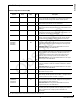
2.0 Pin Description (Continued)
DP83815
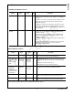
Note: DP83815 supports NM27LV010 for the BIOS ROM interface device.
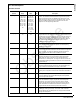
100BASE-TX/10BASE-T Interface
Symbol
LQFP Pin
No(s)
LBGA Pin
No(s) Dir Description
TPTDP, TPTDM 54, 53 G1, F1 A-O Transmit Data: Differential common output driver. This differential
common output is configurable to either 10BASE-T or 100BASE-TX
signaling:
10BASE-T: Transmission of Manchester encoded 10BASE-T packet
data as well as Link Pulses (including Fast Link Pulses for Auto-
Negotiation purposes).
100BASE-TX: Transmission of ANSI X3T12 compliant MLT-3 data.
The DP83815 will automatically configure this common output driver
for the proper signal type as a result of either forced configuration or
Auto-Negotiation.
TPRDP,
TPRDM
46, 45 D1, C1 A-I Receive Data: Differential common input buffer. This differential
common input can be configured to accept either 100BASE-TX or
10BASE-T signaling:
10BASE-T: Reception of Manchester encoded 10BASE-T packet
data as well as normal Link Pulses and Fast Link Pulses for Auto-
Negotiation purposes.
100BASE-TX: Reception of ANSI X3T12 compliant scrambled MLT-3
data.
The DP83815 will automatically configure this common input buffer
to accept the proper signal type as a result of either forced
configuration or Auto-Negotiation.
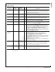
BIOS ROM/Flash Interface
Symbol
LQFP Pin
No(s)
LBGA Pin
No(s) Dir Description
MCSN 129 G13 O BIOS ROM/Flash Chip Select: During a BIOS ROM/Flash
access, this signal is used to select the ROM device.
MD7, MD6, MD5,
MD4/EEDO, MD3,
MD2,
MD1/CFGDISN,
MD0
141, 140, 139,
138, 135, 134,
133, 132
D13, D12,
D14, E11,
E14, F11,
F13, F12
I/O BIOS ROM/Flash Data Bus: During a BIOS ROM/Flash access
these signals are used to transfer data to or from the ROM/Flash
device.
MD[5:0] pins have internal weak pull ups.
MD6 and MD7 pins have internal weak pull downs.
MA5,
MA4/EECLK,
MA3/EEDI,
MA2/LED100LNK,
MA1/LED10LNK,
MA0/LEDACT
3, 2, 1, 144,
143, 142
B11, A12,
B12, C13,
C12, C14
O BIOS ROM/Flash Address: During a BIOS ROM/Flash access,
these signals are used to drive the ROM/Flash address.
MWRN 131 F14 O BIOS ROM/Flash Write: During a BIOS ROM/Flash access, this
signal is used to enable data to be written to the Flash device.
MRDN 130 G11 O BIOS ROM/Flash Read: During a BIOS ROM/Flash access, this
signal is used to enable data to be read from the Flash device.
Obsolete