
Datasheet

6 www.national.com
DP83815
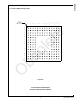
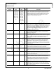
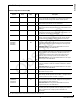
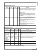
2.0 Pin Description
PCI Bus Interface
Symbol
LQFP Pin
No(s)
LBGA Pin
No(s) Dir Description
AD[31-0] 66, 67, 68, 70,
71, 72, 73, 74,
78, 79, 81, 82,
83, 86, 87, 88,
101, 102, 104,
105, 106, 108,
109, 110, 112,
113, 115, 116,
118, 119, 120,
121
K3, K2, K4,
L3, L2, M1,
N3, P3, L4
N5, M5, L5,
N6, L6, N7,
P7, N10, L10,
M11, N11,
P12, N12,
M13, M14,
L12, L14,
K13, K14,
K11, J13, J14,
J12
I/O Address and Data: Multiplexed address and data bus. As a bus
master, the DP83815 will drive address during the first bus phase.
During subsequent phases, the DP83815 will either read or write
data expecting the target to increment its address pointer. As a bus
target, the DP83815 will decode each address on the bus and
respond if it is the target being addressed.
CBEN[3-0] 75, 89, 100,
111
N4, L7, M10,
L13
I/O Bus Command/Byte Enable: During the address phase these
signals define the “bus command” or the type of bus transaction that
will take place. During the data phase these pins indicate which byte
lanes contain valid data. CBEN[0] applies to byte 0 (bits 7-0) and
CBEN[3] applies to byte 3 (bits 31-24) in the Little Endian Mode. In
Big Endian Mode, CBEN[3] applies to byte 0 (bits 31-24) and
CBEN[0] applies to byte 3 (bits 7-0).
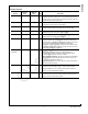
PCICLK 60 H4 I Clock: This PCI Bus clock provides timing for all bus phases. The
rising edge defines the start of each phase. The clock frequency
ranges from 0 to 33 MHz.
DEVSELN 95 P9 I/O Device Select: As a bus master, the DP83815 samples this signal to
insure that the destination address for the data transfer is recognized
by a PCI target. As a target, the DP83815 asserts this signal low
when it recognizes its address after FRAMEN is asserted.
FRAMEN 91 M7 I/O Frame: As a bus master, this signal is asserted low to indicate the
beginning and duration of a bus transaction. Data transfer takes
place when this signal is asserted. It is de-asserted before the
transaction is in its final phase. As a target, the device monitors this
signal before decoding the address to check if the current transaction
is addressed to it.
GNTN 63 J2 I Grant: This signal is asserted low to indicate to the DP83815 that it
has been granted ownership of the bus by the central arbiter. This
input is used when the DP83815 is acting as a bus master.
IDSEL 76 M4 I Initialization Device Select: This pin is sampled by the DP83815 to
identify when configuration read and write accesses are intended for
it.
INTAN 61 J1 O Interrupt A: This signal is asserted low when an interrupt condition
occurs as defined in the Interrupt Status Register, Interrupt Mask,
and Interrupt Enable registers.
IRDYN 92 P8 I/O Initiator Ready: As a bus master, this signal will be asserted low
when the DP83815 is ready to complete the current data phase
transaction. This signal is used in conjunction with the TRYDN
signal. Data transaction takes place at the rising edge of PCICLK
when both IRDYN and TRDYN are asserted low. As a target, this
signal indicates that the master has put the data on the bus.
PAR 99 P10 I/O Parity: This signal indicates even parity across AD[31-0] and
CBEN[3-0] including the PAR pin. As a master, PAR is asserted
during address and write data phases. As a target, PAR is asserted
during read data phases.
Obsolete