
Datasheet
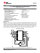
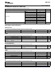
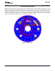


PWP PACKAGE
(TOP VIEW)
FS
FG
RD
VCP
CPP
CPN
W
GND
V
U
VCC
V5
COM
CS
FR
PWMIN
DRV11873
www.ti.com
SLWS237 –NOVEMBER 2012
PIN DESIGNATION
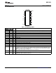
Table 1. PIN DESCRIPTIONS
TERMINAL
I/O
(1)
DESCRIPTION
NAME NO.
FS 1 I Motor parameter adjustment pin. Pull low for lower speed motor and pull high for high speed motor.
FG 2 O Frequency generator output. The output have period equal to 6 electrical states (FG).
RD 3 O In the lock condition, RD output high through a pull up resistor to V
CC
or 5 V.
VCP 4 O Charge pump output
CPP 5 O Charge pump conversion terminal
CPN 6 O Charge pump conversion terminal
W 7 O Phase W output
GND 8 - Ground pin
V 9 O Phase V output
U 10 O Phase U output
VCC 11 I Input voltage for motor and chip supply voltage
V5 12 O 5-V regulator output
COM 13 I Motor common terminal input
Over current threshold set up pin. A resistor set up current limit is connected between this pin and ground.
The voltage across the resistor will compare with the voltage converted from the bottom MOSFETs current.
CS 14 I If MOSFETs current is high, the part will get into the over-current protection mode by turning off top PWM
MOSFET and keeping the bottom MOSFET on.
I
limit
(A) = 6600/R
CS
(Ω), Equation valid range: 500 mA < I
limit
< 2000 mA
FR 15 I Set high for reverse rotation. Set low or floating for forward rotation.
PWM input pin. The PWM input signal will be converted to a fixed switching frequency on MOSFET driver.
PWMIN 16 I
The PWM input signal resolution is less than 1%.
(1) I = input, O = output, N/A = not available
Copyright © 2012, Texas Instruments Incorporated Submit Documentation Feedback 3