
Datasheet

"#$%
SBVS070B − JUNE 2006 − REVISED MAY 2009
www.ti.com
5
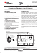
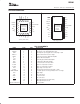
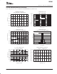
PIN CONFIGURATIONS
Top View RGW Top View DWP
ERROR
DEMAG
GAIN
REF
OUT
REF
IN
V
DD1
OVER−RANGE
CCdiag
V
DD2
I
COMP1
Exposed
Thermal Pad
on Underside,
Connect
to GND1
PWM
PWM
IS1
GND1
IS2
V
OUT
IA
IN2
IA
IN1
GND2
I
COMP2
6
7
8
9
10
1
2
3
4
5
15
14
13
12
11
20
19
18
17
16
QFN−20 (5mm x 5mm)
PWM
PWM
ERROR
DEMAG
GAIN
REF
OUT
REF
IN
V
OUT
IA
IN2
IA
IN1
IS1
GND1
IS2
V
DD1
OVER−RANGE
CCdiag
V
DD2
I
COMP1
I
COMP2
GND2
1
2
3
4
5
6
7
8
9
10
20
19
18
17
16
15
14
13
12
11
Wide−Body SO−20
Exposed
Thermal Pad
on Underside,
Connect
to GND1
PIN ASSIGNMENTS
NAME RGW DWP DESCRIPTION
ERROR 1 3 Error flag: open-drain output, see the Error Conditions section.
DEMAG 2 4 Control input, see the Demagnetization section.
GAIN 3 5 Control input for open-loop gain: low = normal, high = −8dB.
REF
OUT
4 6 Output for internal 2.5V reference voltage.
REF
IN
5 7 Input for zero reference to differential amplifier.
V
OUT
6 8 Output for differential amplifier.
IA
IN2
7 9 Noninverting input of differential amplifier.
IA
IN1
8 10 Inverting input of differential amplifier.
GND2 9 11 Ground connection. Connect to GND1.
I
COMP2
10 12 Output 2 of compensation coil driver.
I
COMP1
11 13 Output 1 of compensation coil driver.
V
DD2
12 14 Supply voltage. Connect to V
DD1
.
CCdiag 13 15 Control input for wire-break detection: high = enable.
OVER−RANGE 14 16 Open-drain output for over-range indication: low = over-range.
V
DD1
15 17 Supply voltage.
IS2 16 18 Probe connection 2.
GND1 17 19 Ground connection.
IS1 18 20 Probe connection 1.
PWM 19 1 PWM output from probe circuit (inverted).
PWM 20 2 PWM output from probe circuit.
Exposed Thermal Pad — — Connect to GND1.