
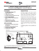
Datasheet


"#$%
SBVS070B − JUNE 2006 − REVISED MAY 2009
www.ti.com
4
ELECTRICAL CHARACTERISTICS (continued)
Boldface limits apply over the specified temperature range, T
J
= −40°C to +125°C, with zero output current I
COMP
.
At T
A
= +25°C and V
DD1
= V
DD2
= +5V with external 100kHz filter BW, unless otherwise noted.
DRV401
PARAMETER CONDITIONS MIN TYP MAX
UNITS
VOLTAGE REFERENCE
Voltage
(2)
No Load 2.495 2.5 2.505 V
Drift
(2)
No Load ±5 ±50 ppm/°C
PSRR
(2)
±15 ±200 µV/V
Load Regulation
(2)
Load to GND/V
DD
, dI = 0mA to 5mA 0.15 mV/mA
Short-Circuit Current I
SC
REF
OUT
Connected to V
DD
+20 mA
REF
OUT
Connected to GND −18 mA
DEMAGNETIZATION
Duration See Timing Diagram 106 130
(3)
ms
DIGITAL I/O
LOGIC INPUTS (DEMAG, GAIN, and CCdiag Pins) CMOS Type Levels
Pull-Up High Current (CCdiag) 3.5 < V
IN
< V
DD
160 µA
Pull-Up Low Current (CCdiag) 0 < V
IN
< 1.5 5 µA
Logic Input Leakage Current 0 < V
IN
< V
DD
0.01 5 µA
Logic Level, Input: L/H 2.1/2.8 V
Hysteresis 0.7 V
OUTPUTS (ERROR AND OVER-RANGE Pins)
Logic Level, Output: L 4mA Sink 0.3 V
Logic Level, Output: H No Internal Pull-Up
OUTPUTS (PWM and PWM Pins) Push-Pull Type
Logic Level L 4mA Sink 0.2 V
Logic Level H 4mA Source (V
DD
) − 0.4 V
POWER SUPPLY
Specified Voltage Range V
DD
4.5 5 5.5 V
Power-On Reset Threshold V
RST
1.8 V
Quiescent Current [I(V
DD1
) + I(V
DD2
)] I
Q
I
COMP
= 0mA, Sensor Not Connected 6.8 mA
Brownout Voltage Level
(2)
4 V
Brownout Indication Delay 135 µs
TEMPERATURE RANGE
Specified Range
T
J
−40 +125 °C
Operating Range
T
J
−50 +150 °C
Package Thermal Resistance
QFN Surface-Mount
q
JA
See Note 6 40 °C/W
SO PowerPAD Surface-Mount
q
JA
See Note 6 27 °C/W
(1)
Parameter value referred to output (RTO).
(2)
See Typical Characteristic curves.
(3)
Total input resistance and comparator threshold current are inversely related. See Figure 2a.
(4)
For VAC sensors, 0.2% of PWM offset approximately corresponds to 10mA primary current offset per winding.
(5)
See Compensation Driver section in Applications Information.
(6)
See Applications Information section for information on power dissipation, layout considerations, and proper PCB soldering and heat-sinking technique.