
Datasheet
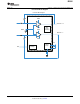

DRV601
www.ti.com
......................................................................................................................................... SLOS553C –JANUARY 2008–REVISED SEPTEMBER 2009
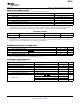
ABSOLUTE MAXIMUM RATINGS
(1)
over operating free-air temperature range, T
A
= 25°C (unless otherwise noted)
VALUE / UNIT
Supply voltage, AVDD, PVDD –0.3 V to 5.5 V
V
I
Input voltage V
SS
– 0.3 V to V
DD
+ 0.3 V
R
(Load)
Minimum load impedance ≥ 100 Ω
T
A
Operating free-air temperature range –40°C to 85°C
T
J
Operating junction temperature range 0°C to 150°C
T
stg
Storage temperature range –65°C to 85°C
(1) Stresses beyond those listed under absolute maximum ratings may cause permanent damage to the device. These are stress ratings
only, and functional operation of the device at these or any other conditions beyond those indicated under recommended operating
conditions is not implied. Exposure to absolute-maximum-rated conditions for extended periods may affect device reliability.
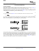
AVAILABLE OPTIONS
T
A
PACKAGED DEVICES
(1)
PART NUMBER SYMBOL
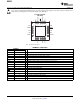
-40°C to 85°C 20-pin, 4 mm × 4 mm QFN DRV601RTJ
(2)
AKQ
(1) For the most current package and ordering information, see the Package Option Addendum at the end of this document, or see the TI
website at www.ti.com.
(2) The RTJ package is only available taped and reeled. To order, add the suffix “R” to the end of the part number for a reel of 3000, or add
the suffix “T” to the end of the part number for a reel of 250 (e.g., DRV601RTJR).
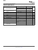
RECOMMENDED OPERATING CONDITIONS
MIN MAX UNIT
V
SS
Supply voltage, AVDD, PVDD 1.8 4.5
(1)
V
V
IH
High-level input voltage SDL, SDR 1.5 V
V
IL
Low-level input voltage SDL, SDR 0.5 V
T
A
Operating free-air temperature –40 85 °C
(1) Device can shut down for V
DD
> 4.5 V to prevent damage to the device.
ELECTRICAL CHARACTERISTICS
T
A
= 25°C (unless otherwise noted)
PARAMETER TEST CONDITIONS MIN TYP MAX UNIT
|V
OS
| Output offset voltage V
DD
= 1.8 V to 4.5 V, Inputs grounded 8 mV
PSRR Power Supply Rejection Ratio V
DD
= 1.8 V to 4.5 V 88 dB
V
OH
High-level output voltage V
DD
= 3.3 V, R
L
= 600 Ω 3.10 V
V
OL
Low-level output voltage V
DD
= 3.3 V, R
L
= 600 Ω –3.05 V
|I
IH
| High-level input current (SDL, SDR) V
DD
= 4.5 V, V
I
= V
DD
1 µA
|I
IL
| Low-level input current (SDL, SDR) V
DD
= 4.5 V, V
I
= 0 V 1 µA
V
DD
= 1.8 V, No load, SDL= SDR = V
DD
5.3
V
DD
= 3.3 V, No load, SDL = SDR = V
DD
7.1 mA
I
DD
Supply Current
V
DD
= 4.5 V, No load, SDL = SDR = V
DD
8.7
Shutdown mode, V
DD
= 1.8 V to 4.5 V 1 µA
Copyright © 2008–2009, Texas Instruments Incorporated 3
Product Folder Link(s): DRV601