
Datasheet


Table Of Contents
DS90CR217
www.ti.com
SNLS226A –OCTOBER 2006–REVISED FEBRUARY 2013
DS90CR217 +3.3V Rising Edge Data Strobe LVDS 21-Bit Channel Link - 85 MHz
Check for Samples: DS90CR217
1
FEATURES
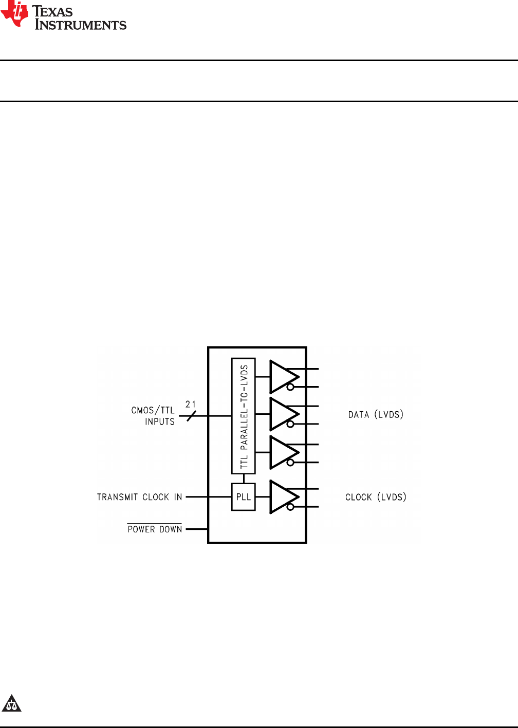
DESCRIPTION
The DS90CR217 transmitter converts 21 bits of
2
• 20 to 85 MHz Shift Clock Support
CMOS/TTL data into three LVDS (Low Voltage
• 50% Duty Cycle on Receiver Output Clock
Differential Signaling) data streams. A phase-locked
• Best-in-Class Set & Hold Times on TxINPUTs
transmit clock is transmitted in parallel with the data
streams over a fourth LVDS link. Every cycle of the
• Low Power Consumption
transmit clock 21 bits of input data are sampled and
• ±1V Common-Mode Range (Around +1.2V)
transmitted. At a transmit clock frequency of 85 MHz,
• Narrow Bus Reduces Cable Size and Cost
21 bits of TTL data are transmitted at a rate of 595
Mbps per LVDS data channel. Using a 85 MHz clock,
• Up to 1.785 Gbps Throughput
the data throughput is 1.785 Gbit/s (223 Mbytes/sec).
• Up to 223 Mbytes/sec Bandwidth
The narrow bus and LVDS signalling of the
• 345 mV (typ) Swing LVDS Devices for Low EMI
DS90CR217 is an ideal means to solve EMI and
• PLL Requires No External Components
cable size problems associated with wide, high-speed
• Rising Edge Data Strobe
TTL interfaces.
• Compatible with TIA/EIA-644 LVDS Standard
• Low Profile 48-Lead TSSOP Package
Block Diagram
Figure 1. DS90CR217
See Package Number DGG0048A
1
Please be aware that an important notice concerning availability, standard warranty, and use in critical applications of
Texas Instruments semiconductor products and disclaimers thereto appears at the end of this data sheet.
2All trademarks are the property of their respective owners.
PRODUCTION DATA information is current as of publication date.
Copyright © 2006–2013, Texas Instruments Incorporated
Products conform to specifications per the terms of the Texas
Instruments standard warranty. Production processing does not
necessarily include testing of all parameters.