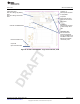
MSP-TS430RGC64B www.ti.com B.17 MSP-TS430RGC64B Figure B-33.
MSP-TS430RGC64B www.ti.com Connector J5 External power connector Jumper JP3 to "ext" Jumpers JP5 to JP10 Close 1-2 to debug in Spy-Bi-Wire mode Close 2-3 to debug in 4-wire JTAG mode If the system should be supplied via LDOI (J6), close JP4 and set JP3 to external Orient Pin 1 of MSP430 device D1 LED connected to P1.0 Jumper JP2 Open to disconnect LED Figure B-34.
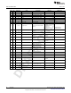
MSP-TS430RGC64B www.ti.com Table B-18. MSP-TS430RGC64B Bill of Materials Pos. Ref Des No. per Board 1 C1, C2 0 12pF, SMD0805 DNP 2 C3, C4 0 47pF, SMD0805 DNP 3 C6, C7, C10 3 10uF/6.3V, SMD0805 4 C5, C11, C13, C14, C15 5 100nF, SMD0805 5 C8 1 2.2nF, SMD0805 6 C9 1 470nF, SMD0805 7 C16 1 4.
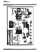
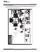
A 13 11 9 7 5 3 1 RST/NMI GND TCK TMS TDI TDO TCK 2 3 1 2 3 JP8 4 THERMAL_4 tbd C4 5 S.G. 9 7 5 3 1 J6 1 2 3 6 J5 0R DVCC 1 2 Size: 0R 1.1 MSP430 Tools TI Friesing Revision: Mentor Pads Logic V9 6 R11 PINHEAD_1X2 JP4 PINHEAD_1X3 GND GND BSL CN-ML10 0 1 8 6 4 2 BOOTST C16 GND C15 4.7uF 1 MSP-TS430RGC64C 100nF GND Comment: PINHEAD_1X3 3 2 1 DVIO Power Circle P1.2/TA0.1 P1.1/TA0.
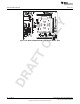
MSP-TS430RGC64C www.ti.com Jumpers JP5 to JP10 Close 1-2 to debug in Spy -Bi-Wire mode Close 2-3 to debug in 4-wire JTAG mode Connector J6 External power connector to supply DVIO Jumper JP4 Close if only one power supply over J5 is used for VCC and DVI Connector J5 External power connector for DVCC. Jumper JP3 to "ext“. Orient Pin 1 of MSP430 device IMPORTANT NOTE: Rev1.0 of the board doesn’t has connection from pin 4 of BOOST to pin 64 of MCU.
MSP-TS430RGC64C www.ti.com Table B-19. MSP-TS430RGC64C Bill of Materials Item Qty Reference 1 0 C1, C2 12pF CAP, SMD, Ceramic, 0805 DNP C1 C2 2 0 C3, C4 tbd CAP, SMD, Ceramic, 0805 DNP C3 C4 4 3 C5, C7, C10 10uF CAP, SMD, Ceramic, 0805 5 5 C8 C6 C13-15 100nF CAP, SMD, Ceramic, 0805 5 5 C8 2.2nF CAP, SMD, Ceramic, 0805 6 1 C9 470nF CAP, SMD, Ceramic, 0805 7 1 C16 4.
MSP-TS430RGC64USB www.ti.com B.19 MSP-TS430RGC64USB Due to the use of diodes in the power chain, the voltage on the MSP430F5xx device is approximately 0.3 V lower than is set by the debugging tool. Set the voltage in the IDE to 0.3 V higher than desired; for example, to run the MCU at 3.0 V, set it to 3.3 V. Figure B-37.
MSP-TS430RGC64USB www.ti.com Figure B-38.
MSP-TS430RGC64USB www.ti.com Table B-20. MSP-TS430RGC64USB Bill of Materials Pos. Ref Des No. Per Board 1 C1, C2 0 12pF, SMD0805 1.1 C3, C4 2 47pF, SMD0805 2 C6, C7 2 10uF/6.3V, Tantal Size B 511-1463-2-ND 3 C5, C11, C13, C14 4 100nF, SMD0805 311-1245-2-ND 3.1 C10, C12 0 10uF, SMD0805 4 C8 1 2.2nF, SMD0805 5 C9 1 470nF, SMD0805 478-1403-2-ND 6 D1 1 green LED, SMD0805 P516TR-ND 7 J1, J2, J3, J4 4 Description DigiKey Part No.
MSP-TS430RGC64USB www.ti.com Table B-20. MSP-TS430RGC64USB Bill of Materials (continued) Ref Des No.
MSP-TS430PN80 www.ti.com B.20 MSP-TS430PN80 NOTE: For MSP430F(G)47x devices: Connect pins 7 and 10 (GND) externally to DVSS (see data sheet). Connect load capacitance on Vref pin 60 when SD16 is used (see data sheet). Figure B-39.
MSP-TS430PN80 www.ti.com LED connected to pin 12 Connector J5 External power connection Remove R8 and jumper R9 Jumper J6 Open to disconnect LED Orient Pin 1 of MSP430 device Figure B-40.
MSP-TS430PN80 www.ti.com Table B-21. MSP-TS430PN80 Bill of Materials Pos. Ref Des No. per Board 1 C1, C2 0 12pF, SMD0805 DNP: C1, C2 1.1 C3, C4 0 47pF, SMD0805 DNP: Only recommendation. Check your crystal spec.
MSP-TS430PN80A www.ti.com B.21 MSP-TS430PN80A Figure B-41.
MSP-TS430PN80A www.ti.com Jumpers JP5 to JP10 Close 1-2 to debug in Spy-Bi-Wire mode Close 2-3 to debug in 4-wire JTAG mode Connector J5 External power connector Jumper JP3 to "ext" Orient Pin 1 of MSP430 device If the system should be supplied via LDOI (J6), close JP4 and set JP3 to external Jumper JP2 Open to disconnect LED D1 LED connected to P1.0 Figure B-42.
MSP-TS430PN80A www.ti.com Table B-22. MSP-TS430PN80A Bill of Materials Position Ref Des No. per Board 1 C1, C2 0 12pF, SMD0805 DNP 2 C3, C4 0 47pF, SMD0805 DNP 3 C6, C7, C10, C12 3 10uF/6.3V, SMD0805 DNP C10 4 C5, C11, C13, C14, C15 5 100nF, SMD0805 5 C8 1 2.2nF, SMD0805 6 C9 1 470nF, SMD0805 7 C16 1 4.
MSP-TS430PN80USB www.ti.com B.22 MSP-TS430PN80USB Due to the use of diodes in the power chain, the voltage on the MSP430F5xx device is approximately 0.3 V lower than is set by the debugging tool. Set the voltage in the IDE to 0.3 V higher than desired; for example, to run the MCU at 3.0 V, set it to 3.3 V. NOTE: R11 should be populated. Figure B-43.
MSP-TS430PN80USB www.ti.com Jumper JP3 1-2 (int): Power supply via JTAG debug interface 2-3 (ext): External power supply USB Connector Jumper JP1 Open to measure current Connector J5 External power connector Jumper JP3 to ‘ext’ Jumper JP4 Close for USB bus powered device Jumper JP5 to JP10 Close 1-2 to debug in Spy-BiWire mode. Close 2-3 to debug in 4-wire JTAG mode. BSL invoke button S3 LED connected to P1.0 Jumper JP2 Open to disconnect LED Figure B-44.
MSP-TS430PN80USB www.ti.com Table B-23. MSP-TS430PN80USB Bill of Materials Pos. Ref Des No. per Board 1 C1, C2 0 12pF, SMD0805 1.1 C3, C4 2 47pF, SMD0805 2 C6, C7 2 10uF/6.3V, Tantal Size B 511-1463-2-ND 3 C5, C11, C13, C14 4 100nF, SMD0805 311-1245-2-ND 3.1 C10, C12 0 10uF, SMD0805 311-1245-2-ND 4 C8 1 2.2nF, SMD0805 5 C9 1 470nF, SMD0805 478-1403-2-ND 6 D1 1 green LED, SMD0805 P516TR-ND 7 J1, J2, J3, J4 7.1 4 Description 20-pin header, TH DigiKey Part No.
MSP-TS430PN80USB www.ti.com Table B-23. MSP-TS430PN80USB Bill of Materials (continued) 100 Pos. Ref Des No. per Board 29 C36 1 10p Buerklin: 56D102 30 C38 1 220n Buerklin: 53D2074 31 C39 1 4u7 Buerklin: 53D2086 32 C40 1 0.
MSP-TS430PZ100 www.ti.com B.23 MSP-TS430PZ100 NOTE: Connections between the JTAG header and pins XOUT and XIN are no longer required and should not be made. Figure B-45.
MSP-TS430PZ100 www.ti.com Jumper J6 Open to disconnect LED Jumper J7 Open to measure current LED connected to pin 12 Connector J5 External power connection Remove R8 and jumper R9 Orient Pin 1 of MSP430 device Figure B-46.
MSP-TS430PZ100 www.ti.com Table B-24. MSP-TS430PZ100 Bill of Materials Pos. Ref Des No. per Board 1 C1, C2 0 12pF, SMD0805 DNP 1b C3, C4 0 47pF, SMD0805 DNP: Only recommendation. Check your crystal spec.
MSP-TS430PZ100A www.ti.com B.24 MSP-TS430PZ100A Figure B-47.
MSP-TS430PZ100A www.ti.com Jumper JP3 1-2 (int): Power supply via JTAG interface 2-3 (ext): External Power Supply Jumper JP1 Open to measure current Jumper JP2 Open to disconnect LED LED D1 connected to P5.1 Orient Pin 1 of Device Figure B-48.
MSP-TS430PZ100A www.ti.com Table B-25. MSP-TS430PZ100A Bill of Materials Pos. Ref Des No. per Board 1 C1, C2 0 12pF, SMD0805 DNP 1b C3, C4 0 47pF, SMD0805 DNP: Only recommendation. Check your crystal spec.
MSP-TS430PZ100B www.ti.com B.25 MSP-TS430PZ100B Figure B-49.
MSP-TS430PZ100B www.ti.com Connector J5 External power connector Jumper JP1 to "ext" Jumper JP1 Open to measure current Orient Pin 1 of MSP430 device JP11, JP12, JP13 Connect 1-2 to connect AUXVCCx with DVCC or drive AUXVCCx externally Jumpers JP5 to JP10 Close 1-2 to debug in Spy-Bi-Wire mode Close 2-3 to debug in 4-wire JTAG mode D1 LED connected to P1.0 Jumper JP2 Open to disconnect LED Figure B-50.
MSP-TS430PZ100B www.ti.com Table B-26. MSP-TS430PZ100B Bill of Materials Ref Des No. per Board 1 C1, C2 0 12pF, SMD0805 2 C4, C5, C6 , C7, C8, C9 6 100nF, SMD0805 311-1245-2-ND 3 C10, C26 2 470 nF, SMD0805 478-1403-2-ND 4 C11, C12 1 10 uF / 6.3 V SMD0805 5 C13, C14, C16, C18, C19, C29 6 4.7 uF SMD0805 6 D1 1 green LED, SMD0805 P516TR-ND 7 J1, J2, J3, J4 0 25-pin header, TH SAM1029-25-ND (Header) SAM1213-25ND (Receptacle) DNP: Headers and receptacles enclosed with kit.
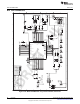
BOOTST 10 8 6 4 2 R10 R11 JTAG DNP DNP 13 11 9 7 5 3 1 0R 0R LDOO C18 100nF C19 100nF GND 1 JP5 2 3 DNP GND JP6 R9 XT2IN R12 XT2OUT TDO 1 RST 2 RST/NMI 3 1 JP4 2 LDOI/LDOO Interface GND R7 330R VCC GND TEST/SBWTCK TCK 1 J6 2 3 Note: If the system should be supplied via LDOI (J6) close JP4 and set JP3 to external LDOI GND RST/NMI TCK TMS TDI TDO RST R5 47K TEST/SBWTCK 2.
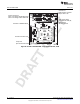
MSP-TS430PZ100C www.ti.
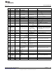
MSP-TS430PZ100C www.ti.com Table B-27. MSP-TS430PZ100C Bill of Materials Pos. Ref Des Number Per Board 1 C1, C2 0 12pF, SMD0805 DNP: C1, C2 1.1 C3, C4 2 47pF, SMD0805 DNP: C3, C4 2 C6, C7 2 10uF/6.3V, Tantal Size B 511-1463-2-ND 3 C5, C11, C13, C14, C19, C20 6 100nF, SMD0805 311-1245-2-ND 3.1 C10, C12, C18,17 0 100nF, SMD0805 311-1245-2-ND 4 C8 1 2.
MSP-TS430PZ100C www.ti.com Table B-27. MSP-TS430PZ100C Bill of Materials (continued) Pos. Ref Des Number Per Board 27 JP11 1 4-pin header, male, TH SAM1035-04-ND 28 C15 1 4.7 uF, SMD0805 Buerklin 53 D 2430 29 C21 1 220nF, SMD0805 Buerklin 53 D 2381 Description Digi-Key Part No.
MSP-TS430PZ5x100 www.ti.com B.27 MSP-TS430PZ5x100 Figure B-53.
MSP-TS430PZ5x100 www.ti.com Jumper JP3 1-2 (int): Power supply via JTAG debug interface 2-3 (ext): External power supply Connector J5 External power connector Jumper J3 to ‘ext’ Jumper JP1 Open to measure current Jumpers JP5 to JP10 Close 1-2 to debug in Spy-Bi-Wire mode. Close 2-3 to debug in 4-wire JTAG mode. LED connected to P1.0 Jumper JP2 Open to disconnect LED Figure B-54.
MSP-TS430PZ5x100 www.ti.com Table B-28. MSP-TS430PZ5x100 Bill of Materials Pos. Ref Des No. per Board 1 C1, C2 0 1b C3, C4 DigiKey Part No. Comment 12pF, SMD0805 DNP 47pF, SMD0805 DNP: Only recommendation. Check your crystal spec. 2 C6, C7 2 10uF/10V, Tantal Size B 511-1463-2-ND 3 C5, C10, C11, C12,C13, C14 4 100nF, SMD0805 311-1245-2-ND 4 C8 0 2.
MSP-TS430PZ100USB www.ti.com B.28 MSP-TS430PZ100USB Due to the use of diodes in the power chain, the voltage on the MSP430F5xx device is approximately 0.3 V lower than is set by the debugging tool. Set the voltage in the IDE to 0.3 V higher than desired; for example, to run the MCU at 3.0 V, set it to 3.3 V. Figure B-55.
MSP-TS430PZ100USB www.ti.com Figure B-56.
MSP-TS430PZ100USB www.ti.com Table B-29. MSP-TS430PZ100USB Bill of Materials Pos. Ref Des No. Per Board 1 C1, C2 0 12pF, SMD0805 1.1 C3, C4 2 47pF, SMD0805 2 C6, C7 2 10uF/6.3V, Tantal Size B 511-1463-2-ND 3 C5, C11, C13, C14, C19 5 100nF, SMD0805 311-1245-2-ND 3.1 C10, C12, C18,17 0 100nF, SMD0805 311-1245-2-ND 4 C8 1 2.2nF, SMD0805 5 C9 1 470nF, SMD0805 478-1403-2-ND 6 D1 1 green LED, SMD0805 P516TR-ND 7 J1, J2, J3, J4 7.
MSP-TS430PZ100USB www.ti.com Table B-29. MSP-TS430PZ100USB Bill of Materials (continued) 120 Pos. Ref Des No. Per Board 30 C38 1 220n SMD0603 Buerklin: 53D2074 31 C39 1 4u7 SMD0603 Buerklin: 53D2086 32 C40 1 0.
EM430F5137RF900 www.ti.com B.29 EM430F5137RF900 (May be addedclose to therespective pins to reduce emissions at 5GHz tole vel required byETSI) Power Management VCC01 = external VCC = AVDD_RF / AVCC_RF = DVCC Vdda1 = AVCC Copyright © 2009–2012, Texas Instruments Incorporated 121 Hardware SLAU278I – May 2009 – Revised May 2012 Submit Documentation Feedback Vdd Vdda2 Port connectors CON1 .. CON3 = Port1 ..
EM430F5137RF900 www.ti.com JTAG connector Jumper JP2 Close EXT for external supply Close INT for JTAG supply Open to measure current jumper JP3 External power connector CON12 Jumper JP1 Spy-Bi-Wire mode VCC GND GND Jumper JP1 Close JTAG position to debug in JTAG mode Open to disconnect LEDs jumper JP5/JP10 LED D2 (red) connected to P3.6 via JP10 LED D1 (green) connected to P1.0 via JP5 Close SBW position to debug in Spy-Bi-Wire mode Push-button S2 connected to P1.
EM430F5137RF900 www.ti.com Table B-30. EM430F5137RF900 Bill of Materials Item Reference No. per Board Description Value 1 Q1 1 ( CUSTOMER SUPPLY ) CRYSTAL, SMT, 4P, 26MHz 26M ASX-531(CS) AKER ELECTRONIC 2 C1-C5, C082, C222, C271, C281, C311, C321, C341, C412, C452 14 CAPACITOR, SMT, 0402, CER, 16V, 10%, 0.1uF 0.1uF 0402YC104KAT2 A AVX 3 C071 1 CAPACITOR, SMT, 0603, CERAMIC, 0.47uF, 16V, 10%, X5R 0.47uF 0603YD474KAT2 A AVX 4 R401 1 RES0402, 47.
EM430F5137RF900 www.ti.com Table B-30. EM430F5137RF900 Bill of Materials (continued) 124 Item Reference No.
EM430F6137RF900 www.ti.com B.30 EM430F6137RF900 (May beaddedclose to therespective pins to reduce emissions at 5GHz to el vel required by ETSI) Power Management VCC01 = external VCC = AVCC = AVDD_RF / AVCC_RF = DVCC Vdda1 Copyright © 2009–2012, Texas Instruments Incorporated 125 Hardware SLAU278I – May 2009 – Revised May 2012 Submit Documentation Feedback Vdd Vdda2 Port connectors CON1 .. CON5 = Port1 ..
EM430F6137RF900 www.ti.com JTAG connector Jumper JP2 Close EXT for external supply Close INT for JTAG supply Open to measure current jumper JP3 External power connector CON12 Jumper JP1 Spy-Bi-Wire mode VCC GND GND Jumper JP1 Close JTAG position to debug in JTAG mode Open to disconnect LEDs jumper JP5/JP10 LED D2 (red) connected to P3.6 via JP10 Close SBW position to debug in Spy-Bi-Wire mode Push-button S2 connected to P1.7 LED D1 (green) connected to P1.
EM430F6137RF900 www.ti.com Table B-31. EM430F6137RF900 Bill of Materials Pos. Ref Des No. per Board 1 Q1 1 ( CUSTOMER SUPPLY ) CRYSTAL, SMT, 4P, 26MHz ASX-531(CS) AKER ELECTRONIC 2 C1-C5, C112, C252, C381, C391, C421, C431, C451, C522, C562 14 CAPACITOR, SMT, 0402, CER, 16V, 10%, 0.1uF 0402YC104KAT2A AVX 3 C101 1 CAPACITOR, SMT, 0603, CERAMIC, 0.47uF, 0603YD474KAT2A 16V, 10%, X5R AVX 4 R511 1 RES0402, 47.0K CRCW04024702F100 DALE 09 18 514 6323 HARTING Description Part No.
EM430F6137RF900 www.ti.com Table B-31. EM430F6137RF900 Bill of Materials (continued) 128 Pos. Ref Des No. per Board 33 U1 1 DUT, SMT, PQFP, RGC-64, 0.5mmLS, 9.15x9.15x1mm, THRM.PAD CC430F6137 TI 34 JP1 1 Pin Connector 2x4pin 61300821121 WUERTH Description Part No.
EM430F6147RF900 www.ti.com B.31 EM430F6147RF900 Figure B-61.
EM430F6147RF900 www.ti.com Figure B-62.
EM430F6147RF900 www.ti.com Table B-32. EM430F6147RF900 Bill of Materials Pos. Ref Des No. per Board 1 Q1 1 ( CUSTOMER SUPPLY ) CRYSTAL, SMT, 4P, 26MHz ASX-531(CS) AKER ELECTRONIC 2 C1-5 C112 C252 C381 C391 C421 C431 C451 C522 C562 14 CAPACITOR, SMT, 0402, CER, 16V, 10%, 0.1uF 0402YC104KAT2A AVX 3 C101 1 CAPACITOR, SMT, 0603, CERAMIC, 0.47uF, 0603YD474KAT2A 16V, 10%, X5R AVX 4 R511 1 RES0402, 47.0K CRCW04024702F100 DALE 09 18 514 6323 HARTING Description Part No.
EM430F6147RF900 www.ti.com Table B-32. EM430F6147RF900 Bill of Materials (continued) Pos. Ref Des No. per Board 31 U1 1 DUT, SMT, PQFP, RGC-64, 0.5mmLS, 9.15x9.15x1mm, THRM.
MSP-FET430PIF www.ti.com B.32 MSP-FET430PIF Figure B-63.
MSP-FET430PIF www.ti.com Figure B-64.
MSP-FET430UIF www.ti.com B.33 MSP-FET430UIF Figure B-65.
MSP-FET430UIF www.ti.com Figure B-66.
MSP-FET430UIF www.ti.com Figure B-67.
MSP-FET430UIF www.ti.com Figure B-68.
MSP-FET430UIF www.ti.com Figure B-69.
MSP-FET430UIF www.ti.com B.33.1 MSP-FET430UIF Revision History Revision 1.3 • Initial released hardware version Assembly change on 1.3 (May 2005) • R29, R51, R42, R21, R22, R74: value changed from 330R to 100R Changes 1.3 to 1.4 (Aug 2005) • J5: VBUS and RESET additionally connected • R29, R51, R42, R21, R22, R74: value changed from 330R to 100R • U1, U7: F1612 can reset TUSB3410; R44 = 0R added • TARGET-CON.
Appendix C SLAU278I – May 2009 – Revised May 2012 Hardware Installation Guide This section describes the hardware installation process of the following USB debug interfaces on a PC running Windows XP: • MSP-FET430UIF • eZ430-F2013 • eZ430-RF2500 • eZ430-Chronos • eZ430-RF2780 • eZ430-RF2560 • MSP-WDSxx "Metawatch" • LaunchPad (MSP-EXP430G2) • MSP-EXP430FR5739 • MSP-EXP430F5529 The installation procedure for other supported versions of Windows is very similar and, therefore, not shown here. Topic C.1 ...
Hardware Installation C.1 www.ti.com Hardware Installation Table C-1 shows the USB VIDs and PIDs used in MSP430 tools. Table C-1. USB VIDs and PIDs Used in MSP430 Tools USB VID USB PID INF File Name eZ430-F2013 Tool 0x0451 0xF430 usbuart3410.inf eZ430-RF2500 0x0451 0xF432 430CDC.inf eZ430-RF2780 0x0451 0xF432 430CDC.inf eZ430-RF2560 0x0451 0xF432 430CDC.inf MSP-WDSxx "Metawatch" 0x0451 0xF432 430CDC.inf eZ430-Chronos 0x0451 0xF432 430CDC.
Hardware Installation www.ti.com 4. Browse to the folder where the driver information files are located (see Figure C-2). For CCS, the default folder is: c:\ti\ccsv5\ccs_base\emulation\drivers\msp430\USB_CDC, or c:\ti\ccsv5\ccs_base\emulation\drivers\msp430\USB_FET_XP_XX, or c:\ti\ccsv5\ccs_base\emulation\drivers\msp430\USB_eZ-RF depending of firmware version of the tool. For IAR Embedded Workbench, the default folder is: \Embedded Workbench x.x\ 430\drivers\TIUSBFET\eZ430-UART, or
Hardware Installation www.ti.com 6. The wizard installs the driver files. 7. The wizard shows a message that it has finished the installation of the software USB Debug Interface. 8. The USB debug interface is installed and ready to use. The Device Manager lists a new entry as shown in Figure C-3, Figure C-4, or Figure C-5. Figure C-3.
Hardware Installation www.ti.com Figure C-4.
Hardware Installation www.ti.com Figure C-5.
Document Revision History www.ti.com Document Revision History Version SLAU278 Changes Initial release SLAU278A Updated USB driver installation according to CCE v3.1 SR1 and CCS v4. SLAU278B Added information about MSP-FET430U80USB, MSP-TS430PN80USB, and eZ430-Chronos. SLAU278C Added bills of materials and updated some PCBs in Appendix B. Added information about MSP-TS430DA38, MSP-TS430DL48, MSP-TS430PW14, MSP-TS430PW28.
RF EMISSION TESTING All MSP-TS430XXX kits and kits listed below have been tested for compliance with Part 15 of the FCC and Canadian ICES-003 rules. See REGULATORY COMPLIANCE INFORMATION for details on compliance with these rules. All other kits described in this document either have not been tested or have the statement in their documentation, which is listed in Related Documentation From Texas Instruments.
FCC Interference Statement for Class B EVM devices This equipment has been tested and found to comply with the limits for a Class B digital device, pursuant to part 15 of the FCC Rules. These limits are designed to provide reasonable protection against harmful interference in a residential installation. This equipment generates, uses and can radiate radio frequency energy and, if not installed and used in accordance with the instructions, may cause harmful interference to radio communications.
EVALUATION BOARD/KIT/MODULE (EVM) WARNINGS, RESTRICTIONS AND DISCLAIMERS For Feasibility Evaluation Only, in Laboratory/Development Environments. Unless otherwise indicated, this EVM is not a finished electrical equipment and not intended for consumer use.