User's Guide SLAU204 – December 2006 DAC8555EVM User's Guide This user’s guide describes the characteristics, operation and use of the DAC8555 Evaluation Module (EVM). It covers all matters related to proper use and configuration of this EVM along with the devices that it supports. The physical printed circuit board (PCB) layout, schematic diagram and circuit descriptions are also included.
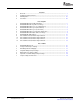
www.ti.com 1 2 3 4 Contents Overview ............................................................................................. 3 PCB Design and Performance .................................................................... 6 EVM Operation .................................................................................... 16 Schematic ..........................................................................................
www.ti.com Overview 1 Overview This section gives a general overview of the DAC8555EVM and describes some of the factors that must be considered when using this demonstration board. 1.1 Features The DAC8555EVM is a simple evaluation module designed for a quick and easy way to evaluate the functionality and performance of the high-resolution, quad-channel, serial input DAC8555 digital-to-analog converter (DAC).
www.ti.com Overview CAUTION When applying an external voltage reference through TP2 or J4-20, make sure that it does not exceed +5V maximum. External voltage references in excess of +5V can permanently damage the DAC8555 being tested (U1). 1.3 EVM Basic Functions The DAC8555EVM is designed to provide a demonstration platform for testing certain operational characteristics of the DAC8555 digital-to-analog converter.
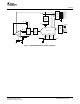
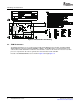
www.ti.com Overview VCC VSS +3.3VA VDD External Reference Module VCC GND VSS GND VDD +5VA +3.3VA (J1) (J5) (J3A) (J3B) +5VA JMP16 JMP8 TP2 JMP15 DAC Out Output Buffer Module (J4A) (J4B) 8 CH JMP11 JMP12 JMP13 JMP14 (J2A) (J2B) VREFH DAC Module 4 CH RST RSTSEL RSTSEL RST EN DIN LDAC SCLK SYNC VREFL JMP5 VREFH JMP6 JMP4 JMP3 TP4 TP3 JMP9 JMP10 VSS Figure 1.
www.ti.com PCB Design and Performance 1.3.1 Related Documentation from Texas Instruments The following documents provide information regarding Texas Instrument integrated circuits used in the assembly of the DAC8555EVM. The latest revisions of these documents are available from the TI web site at http://www.ti.com.
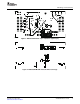
www.ti.com PCB Design and Performance Figure 2. DAC8555EVM PCB—Top Silkscreen Image Figure 3.
www.ti.com PCB Design and Performance Figure 4. DAC8555EVM PCB—Layer 2 (Ground Plane) Figure 5.
www.ti.com PCB Design and Performance Figure 6. DAC8555EVM PCB—Layer 4 (Bottom Signal Layer) Figure 7.
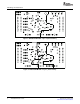
www.ti.com PCB Design and Performance Figure 8. DAC8555EVM—Drill Drawing 2.2 EVM Performance The EVM performance test is executed using a high-density DAC bench test board, an Agilent 3458A digital multimeter and a PC running LabVIEW™ software. The EVM board is tested for linearity for all codes between 485 and 64741. The DUT is then allowed to settle for 1ms before the meter is read. This process is repeated for all codes to generate the measurements for INL and DNL.
www.ti.com PCB Design and Performance Figure 9.
www.ti.com PCB Design and Performance Figure 10.
www.ti.com PCB Design and Performance Figure 11.
www.ti.com PCB Design and Performance Figure 12.
www.ti.com PCB Design and Performance 2.3 Bill of Materials The parts list, showing the components used in the assembly of the DAC8555EVM, is given in Table 1. Table 1.
www.ti.com EVM Operation 3 EVM Operation This section covers the operation of the EVM in detail, in order to provide guidance to the user in evaluating the onboard DAC as well as how to interface the EVM to a specific host processor. Refer to the DAC8555 datasheet for information about its serial interface and other related topics. The EVM board is factory-tested and configured. 3.1 Default Settings The EVM is set to its factory default configuration as described in Table 2 to operate in 5V mode.
www.ti.com EVM Operation Table 3. DAC Output Channel Mapping Reference JMP11 JMP12 JMP13 JMP14 Jumper Position Function 1-2 DAC output A (VOUTA) is routed to J4-2. 2-3 DAC output A (VOUTA) is routed to J4-10. 1-2 DAC output B (VOUTB) is routed to J4-4. 2-3 DAC output B (VOUTB) is routed to J4-12. 1-2 DAC output C (VOUTC) is routed to J4-6. 2-3 DAC output C (VOUTC) is routed to J4-14. 1-2 DAC output D (VOUTD) is routed to J4-8. 2-3 DAC output D (VOUTD) is routed to J4-16.
www.ti.com EVM Operation 3.4.1 Unity Gain Output The buffered output configuration can be used to prevent loading of the DAC8555, though it may add some slight distortion because of the feedback resistor and capacitor. The feedback circuit can be altered by simply desoldering R8 and C12 and replacing them with components of desired value. If desired, R8 and C12 can be removed altogether by replacing R8 with a 0Ω resistor.
www.ti.com EVM Operation 3.4.3 Capacitive Load Drive It may be required to drive a wide range of capacitive loads. However, under certain conditions, all op amps may become unstable, depending on the op amp configuration, gain, and load value. These factors are just few of the issues that can affect op amp stability and should be considered during implementation. In unity gain configuration, the OPA627 op amp (U2) performs very well with very large capacitive loads.
www.ti.com EVM Operation Table 7. Jumper Settings and Functions (continued) Reference Jumper Setting (1) Function RST pin is set high through pull-up resistor R4. RST can be driven by GPIO5, J2-19. JMP4 RST pin is set low. Disconnects VREFH to the inverting input of the op amp U2. JMP5 Connects VREFH to the inverting input of the op amp U2. Disconnects the inverting input of the op amp U2 from the gain resistor, R9.
www.ti.com EVM Operation Table 7. Jumper Settings and Functions (continued) Reference Jumper Setting (1) Function 1 3 Routes VOUTB to J4-4. 1 3 Routes VOUTB to J4-12. 1 3 Routes VOUTC to J4-6. 1 3 Routes VOUTC to J4-14. 1 3 Routes VOUTD to J4-8. 1 3 Routes VOUTD to J4-16. 1 3 Routes J4-1 to U2 noninverting input. 1 3 Routes J4-3 to U2 noninverting input. 1 3 Routes U2 output to J4-5. 1 3 Routes U2 output to J4-7.
www.ti.
REVISION HISTORY REV ENGINEERING CHANGE NUMBER APPROVED JMP7 +5VA +3.3VA 1 2 3 VDD VCC AVDD D R4 10K R5 NI R6 NI 7 R3 10K C5 0.1uF C2 10uF C7 0.
FCC Warning This evaluation board/kit is intended for use for ENGINEERING DEVELOPMENT, DEMONSTRATION, OR EVALUATION PURPOSES ONLY and is not considered by TI to be a finished end-product fit for general customer use. It generates, uses, and can radiate radio frequency energy and has not been tested for compliance with the limits of computing devices pursuant to part 15 of FCC rules, which are designed to provide reasonable protection against radio frequency interference.
IMPORTANT NOTICE Texas Instruments Incorporated and its subsidiaries (TI) reserve the right to make corrections, modifications, enhancements, improvements, and other changes to its products and services at any time and to discontinue any product or service without notice. Customers should obtain the latest relevant information before placing orders and should verify that such information is current and complete.