
Personal Lift User Manual


www.ti.com
3.4.3 Capacitive Load Drive
3.5 Optional Signal Conditioning Op-Amp (U4B)
3.6 Jumper Settings
EVM Operation
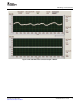
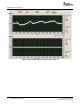
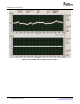
It may be required to drive a wide range of capacitive loads. However, under certain conditions, all op
amps may become unstable, depending on the op amp configuration, gain, and load value. These factors
are just few of the issues that can affect op amp stability and should be considered during implementation.
In unity gain configuration, the OPA627 op amp (U2) performs very well with very large capacitive loads.
Increasing the gain enhances amplifier ability to drive even more capacitance, and adding a load resistor
even improves the capacitive load drive capability.
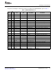
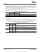
Table 6 shows the jumper setting configuration for a capacitive load drive.
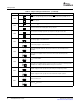
Table 6. Capacitive Load Drive Output Jumper Settings
Jumper Setting
Reference Unipolar Bipolar Function
JMP5 Open Open V
REF
H is disconnected from the inverting input of the output op amp U2.
Supplies power, V
SS
, to the negative rail of op amp U2 for bipolar mode, or ties it to AGND
JMP10 2-3 1-2
for unipolar mode.
Capacitive load drive output of DAC is routed to pin 2 of JMP6 and may be used as the
JMP6 Open Open
output terminal.
One half of the OPA2132 dual package op amp (U4) is used for reference buffering (U4A), while the other
half is unused. This unused op amp (U4B) is left for whatever op amp circuit application the user desires
to implement. The 1206 footprint for the resistors and capacitors surrounding the U4B op amp are not
populated and are made available for easy configuration. Test points TP5 and TP6 are not installed, so it
is up to the user on how to connect the ( ± ) input signals to this op amp. No test point has been made
available for the output because of space restrictions, but a wire can be soldered to the output of the op
amp via an unused component pad that connects to it. The op amp circuit can be configured by populating
the corresponding components to those that match the circuit design while leaving all other unused
component footprints unpopulated.
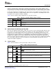
Table 7 shows the function of each specific jumper setting of the EVM.
Table 7. Jumper Settings and Functions
Reference Jumper Setting
(1)
Function
ENABLE pin is set high through pull-up resistor R1. ENABLE can be driven by GPIO2,
J2-8.
JMP1
ENABLE pin is set low and DAC is enabled.
LDAC pin is set high through pull-up resistor R2. LDAC can be driven by GPIO0, J2-2.
JMP2
LDAC pin is set low and DAC update is accomplished via software.
RSTSEL pin is set high through pull-up resistor R3. RSTSEL can be driven by GPIO4,
J2-14.
JMP3
RSTSEL pin is set low.
(1)
Indicates the corresponding pins that are shorted or closed.
SLAU204 – December 2006 DAC8555EVM User's Guide 19
Submit Documentation Feedback