
TV Cables User Manual

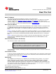
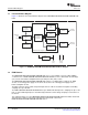

1.1 Functional Block Diagram
CN003
Serial
Connector
I/V
5534a
I/V
5534a
I/V
5534a
I/V
5534a
BALAmp
5534a
BALAmp
5534a
LchOUT
(4.5V )
RMS
RchOUT
(4.5V )
RMS
DAI
CS8414
SW001 003
ModeControl
-
S/PDIFIN
OPT
Coax
DSDS1796
PCM1795
PCM1796
PCM1798
DEM-AS/CDACDaughterCard
3.3-V
Regulator
+VCC
(5V)
±
±
AVCC
( 15V)
1.2 EVM Features
Functional Block Diagram
www.ti.com
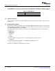
Figure 1-1 illustrates the functional block diagram of the DEM-DSD1796/PCM1795/PCM1796/PCM1798
EVM.
Figure 1-1. DEM-DSD1796/PCM1795/PCM1796/PCM1798 Block Diagram
The DEM-DSD1796/PCM1795/PCM1796/PCM1798 series of stereo DACs consist of a DAI (S/PDIF)
section that uses a DSD1796/PCM1795/PCM1796/PCM1798 DAC section, a differential current/voltage
(I/V) section, and a balanced amplifier with a post-low-pass filter (LPF) section.
The DEM-DSD1796/PCM1795/PCM1796/PCM1798 requires a 5-V digital power supply for its digital
circuits, a 5-V analog power supply for the device itself, and a ± 15-V analog power supply for the
balanced amplifier circuits.
The DAI section has both coaxial and optical inputs that are switch-selectable and capable of handling
sampling rates up to 96 kHz.
The DSD1796/PCM1795/PCM1796/PCM1798 accepts PCM audio data input at a sampling rate up to 192
kHz, or a 64-f
S
DSD signal input, as determined by functional control settings and jumper connections on
the board.
This evaluation fixture uses the DEM-DSD1796/PCM1795/PCM1796/PCM1798 demonstration board and
demonstration software for functional evaluation and operational control of the
DSD1796/PCM1795/PCM1796/PCM1798 DAC device.
Description 8 SLEU057A – September 2004 – Revised May 2009
Submit Documentation Feedback