
User manual


Developing With eZ430-RF2500T Target Board
www.ti.com
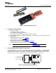
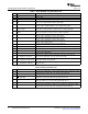
Table 1. eZ430-RF2500T Target Board Pinouts
Pin Function Description
1 GND Ground reference
2 VCC Supply voltage
3 P2.0 / ACLK / A0 / OA0I0 General-purpose digital I/O pin / ACLK output / ADC10, analog input A0
P2.1 / TAINCLK / SMCLK / A1 / General-purpose digital I/O pin / ADC10, analog input A1
4
A0O Timer_A, clock signal at INCLK, SMCLK signal output
General-purpose digital I/O pin / ADC10, analog input A2
5 P2.2 / TA0 / A2 / OA0I1
Timer_A, capture: CCI0B input/BSL receive, compare: OUT0 output
P2.3 / TA1 / A3 / VREF– / VeREF– General-purpose digital I/O pin / Timer_A, capture: CCI1B input, compare: OUT1
6
/ OA1I1 / OA1O output / ADC10, analog input A3 / negative reference voltage output/input
P2.4 / TA2 / A4 / VREF+ / VeREF+ General-purpose digital I/O pin / Timer_A, compare: OUT2 output /
7
/ OA1I0 ADC10, analog input A4 / positive reference voltage output/input
General-purpose digital I/O pin / ADC10 analog input A12 /
8 P4.3 / TB0 / A12 / OA0O
Timer_B, capture: CCI0B input, compare: OUT0 output
General-purpose digital I/O pin / ADC10 analog input A13 /
9 P4.4 / TB1 / A13 / OA1O
Timer_B, capture: CCI1B input, compare: OUT1 output
General-purpose digital I/O pin / ADC10 analog input A14 /
10 P4.5 / TB2 / A14 / OA0I3
Timer_B, compare: OUT2 output
General-purpose digital I/O pin / ADC10 analog input A15 /
11 P4.6 / TBOUTH / A15 / OA1I3
Timer_B, switch all TB0 to TB3 outputs to high impedance
12 GND Ground reference
13 P2.6 / XIN (GDO0) General-purpose digital I/O pin / Input terminal of crystal oscillator
14 P2.7 / XOUT (GDO2) General-purpose digital I/O pin / Output terminal of crystal oscillator
General-purpose digital I/O pin
15 P3.2 / UCB0SOMI / UCB0SCL
USCI_B0 slave out/master in when in SPI mode, SCL I2C clock in I2C mode
General-purpose digital I/O pin
16 P3.3 / UCB0CLK / UCA0STE
USCI_B0 clock input/output / USCI_A0 slave transmit enable
General-purpose digital I/O pin / USCI_B0 slave transmit enable / USCI_A0 clock
17 P3.0 / UCB0STE / UCA0CLK / A5
input/output / ADC10, analog input A5
General-purpose digital I/O pin / USCI_B0 slave in/master out in SPI mode, SDA I2C
18 P3.1 / UCB0SIMO / UCB0SDA
data in I2C mode
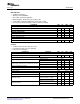
Table 2. Battery Board Pinouts
Pin Function Description
General-purpose digital I/O pin / USCI_A0 transmit data output in UART mode (UART
1 P3.4 / UCA0TXD / UCA0SIMO
communication from 2274 to PC), slave in/master out in SPI mode
2 GND Ground reference
Reset or nonmaskable interrupt input
3 RST / SBWTDIO
Spy-Bi-Wire test data input/output during programming and test
Selects test mode for JTAG pins on Port1. The device protection fuse is connected to
4 TEST / SBWTCK
TEST. Spy-Bi-Wire test clock input during programming and test
5 VCC (3.6V) Supply voltage
General-purpose digital I/O pin / USCI_A0 receive data input in UART mode (UART
6 P3.5 / UCA0RXD / UCA0SOMI
communication from 2274 to PC), slave out/master in when in SPI mode
8 eZ430-RF2500 Development Tool SLAU227E – September 2007 – Revised April 2009
Submit Documentation Feedback