FPD-Link Evaluation Kit User’s Manual FPD-Link Evaluation Kit User’s Manual NSID FLINK3V8BT-85 Rev 3.0 National Semiconductor Corporation Rev 3.
FPD-Link Evaluation Kit User’s Manual Table of Contents INTRODUCTION .............................................................................................................. 3 CONTENTS OF EVALUATION KIT................................................................................. 4 APPLICATIONS ............................................................................................................... 4 FEATURES AND EXPLANATIONS ..................................................................
FPD-Link Evaluation Kit User’s Manual Introduction: National Semiconductor - Interface Products Group FPD-Link evaluation kit contains a Transmitter (Tx) board, a Receiver (Rx) board along with interfacing cables. This kit will demonstrate the DS90C385A/DS90CF386 chipsets interfacing from test equipment or a graphics controller using Low Voltage Differential Signaling (LVDS) to a receiver board. The Transmitter board accepts LVTTL/LVCMOS RGB signals from the graphics controller along with the clock signal.
FPD-Link Evaluation Kit User’s Manual Contents of the Evaluation Kit: 1) One Transmitter board with the DS90C385AMTD - 28 bit Transmitter 2) One Receiver board with the DS90CF386MTD - 28 bit Receiver 3) One 20-pin IDC Flat Ribbon Cable 4) One 60-pin IDC Flat Ribbon Cable 5) Evaluation Kit Documentation (this manual) 6) DS90C385A/DS90CF386 Datasheet 7) LVDS Owner’s Manual (2nd Edition) FPD-Link Typical Application: DATA (LVDS) HOST GRAPHICS CONTROLLER LVCMOS/ LVTTL LVCMOS/ LVTTL LCD PANEL CONTROLLER C
FPD-Link Evaluation Kit User’s Manual Chipsets support up to 18-bit or 24-bit AM-TFT LCD Panels for any VGA (640X480), SVGA (800X600), XGA (1024X768), and Single/Dual Pixel SXGA (1280X1024) resolutions. Because of the non-periodic nature of STN-DD SHFCLK, the Chipset may not work with all D-STN panels. The PLL CLK input of the Transmitter requires a free running periodic SHFCLK. Most Graphics Controller can provide a separate pin with a free running clock.
FPD-Link Evaluation Kit User’s Manual How to set up the Evaluation Kit: The PCB routing for the Tx input pins (TxIN) have been laid out to accept incoming data from a 60-pin IDC connector. The TxOUT/RxIN interface uses a 20-pin IDC connector through a IDC ribbon cable. Please follow these steps to set up the evaluation kit for bench testing and performance measurements: 1) Connect one end of the 20-pin IDC cable to the transmitter board and the other end to the receiver board. Longer lengths can be used.
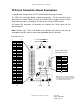
FPD-Link Evaluation Kit User’s Manual FPD-Link Transmitter Board Description: J1 (60 position) accepts 28 bit LVTTL/LVCMOS data along with the clock. The FPD-Link Transmitter board is powered externally. For the transmitter to be operational, the Power Down pin must be set HIGH with a jumper. Rising or falling edge reference clock is selected by JP1 tied to Vcc (rising) or GND (falling). The 20-pin IDC connector (J2) provides the interface for LVDS signals for the Receiver board.
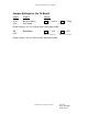
FPD-Link Evaluation Kit User’s Manual Jumper Settings for the Tx Board Jumper Purpose Settings R_FB (JP1) Rising or Falling Data Strobe Vcc = Rising GND = Falling Vcc GND Default setting is JP1 set LOW (to GND), falling edge strobe. /PD (JP2) PowerDown = ON Vcc GND (ON: Tx is operational; = OFF Vcc GND OFF: Tx powers down) Default setting is JP2 set HIGH (to Vcc), operational mode. National Semiconductor Corporation Rev 3.
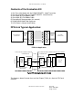
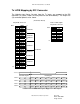
FPD-Link Evaluation Kit User’s Manual Tx LVDS Mapping by IDC Connector The following two figures illustrate how the Tx inputs are mapped to the IDC connector (J1) (Note – labels are also printed on the demo boards). The 20-pin IDC (J2) connector pinout is also shown.
FPD-Link Evaluation Kit User’s Manual Tx Board Options: 50 Ohm Termination for TxIN On the Tx demo board, the 29 inputs have an option for 50 Ohm terminations. There are 0402 pads for this purpose. One side is connected to the signal line and the other side is tied to ground. These pads are unpopulated from the factory but are provided if the user needs to install a 50 Ohm termination. R1 TO R28 are associated with the Tx data input lines. R29 is associated with CLKIN.
FPD-Link Evaluation Kit User’s Manual BOM (Bill of Materials) Transmitter PCB: HSL Demo Board Schematic REV3 HSL8TXR3 Revision: 3 FPD-Link Item Qty Reference Part Pkg Size 1 1 C1 10 µF CASE D 2 4 C2,C6,C10,C14 0.1 µF 1206 (3216) 3 4 C3,C7,C11,C15 22 µF 7343 (D) 4 3 C4,C8,C12 0.001 µF 0805 (2012) 5 3 C5,C9,C13 0.01 µF 0805 (2012) 6 2 JP2,JP1 3_PIN_HEADER 0.
FPD-Link Evaluation Kit User’s Manual Rx FPD-Link Receiver Board: J1 (60 position) provides access to the 28 bit LVTTL/LVCMOS and clock outputs. The FPD-Link Receiver board is powered from the pads show below. For the receiver to be operational, the Power Down pin must be set HIGH with the jumper. The 20-pin IDC connector (J2) provides the interface for LVDS signals for the Receiver board.
FPD-Link Evaluation Kit User’s Manual Selectable Jumper Settings for the Rx Board Jumper Purpose /PD (JP1) PowerDown Settings = ON Vcc GND (ON: Rx is operational; = OFF Vcc GND OFF: Rx powers down) Default setting is JP1 set HIGH (to Vcc), operational mode. National Semiconductor Corporation Rev 3.
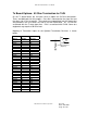
FPD-Link Evaluation Kit User’s Manual LVDS Mapping by IDC Connector The following two figures illustrate how the Rx outputs are mapped to the IDC connector (J1) (Note – labels are also printed on the demo boards). The 20-pin IDC connector (J2) pinout is also shown.
FPD-Link Evaluation Kit User’s Manual Rx Optional: Series Termination for RxOut On the Rx demo board, there are 29 outputs that have an 0402 pad in series (which are shorted out). These pads are unpopulated from the factory but are provided if the user needs to install a 450 Ohm series resistors. This is required if directly connecting to 50 Ohm inputs on a scope. To use this option the user must cut the signal line between the pads before installing the 450 Ohm series resistors.
FPD-Link Evaluation Kit User’s Manual BOM (Bill of Materials) Receiver PCB: HSL Demo Board Schematic REV3 HSL8RXR3 Revision: 3 FPD-Link Item Qty Reference Part Pkg Size 1 1 C1 10 µF CASE D 2 4 C2,C6,C10,C14 0.1 µF 1206 (3216) 3 4 C3,C7,C11,C15 22 µF 7343 (D) 4 3 C4,C8,C12 0.001 µF 0805 (2012) 5 3 C5,C9,C13 0.01 µF 0805 (2012) 6 1 JP1 3_PIN_HEADER 0.
FPD-Link Evaluation Kit User’s Manual Typical Connection / Test Equipment The following is a list of typical test equipment that may be used to generate signals for the TX inputs: 1) Graphics card or GUI controller with digital RGB (LVTTL) output. 2) TEK HFS9009 - This pattern generator along with 9DG2 Cards may be used to generate input signals and also the clock signal. 3) TEK DG2020 - This generator may also be used to generate data and clock signals.
FPD-Link Evaluation Kit User’s Manual The picture below shows a typical test set up using a generator and scope. Signal/Pattern Generator, BERT Tester Optional Termination Transmitter Board Receiver Board 50 ohm 50 ohm 450 ohm 50 ohm LVDS Interface Cable 50 ohm Optional Termination Oscilloscope, BERT Tester Typical Connection / Test Equipment Setup National Semiconductor Corporation Rev 3.
FPD-Link Evaluation Kit User’s Manual Typical Waveshapes LVDS The plot above shows both the LVDS Data channel with PRBS data and also the LVDS Clock over laid. Note that the clock pattern is 4 bit times HIGH and 3 bit times LOW. The differential signal should be typically +/-300mV. These waveforms were acquired using the TEK P6248 Probes. Clock rate is 85MHz. National Semiconductor Corporation Rev 3.
FPD-Link Evaluation Kit User’s Manual RxOUT The plot above shows both the recovered PRBS data and also the regenerated Clock overlaid. Note that the clock transitions slightly before the data transition and strobes the data on the falling edge of the clock. The data and clock signals are low drive 3V CMOS outputs. The plot above is at 85MHz. National Semiconductor Corporation Rev 3.
FPD-Link Evaluation Kit User’s Manual Troubleshooting If the demo boards are not performing properly, use the following as a guide for quick solutions to potential problems. QUICK CHECKS: 1. Check that Power and Ground are connected to both Tx AND Rx boards. 2. Check the supply voltage (typical 3.3V) and also current draw with both Tx and Rx boards (should be about 200mA with clock and one data bit at 66MHz). 3.
FPD-Link Evaluation Kit User’s Manual Additional Information For more information on FPD-Link Transmitters/Receivers, refer to the National’s LVDS website at: www.national.
FPD-Link Evaluation Kit User’s Manual Appendix Tx PCB Schematic Transmitter Board: HSL Demo Board Schematic Document Number: HSL8TXR3 Rev: 3.0 Rx PCB Schematic Receiver Board: HSL Demo Board Schematic Document Number: HSL8RXR3 Rev: 3.0 National Semiconductor Corporation Rev 3.
+3.
+3.6V MAX VCC U1 LVDS_GND RXIN0+ RXIN1+ RXIN2+ RXCLKIN+ RXIN3+ J2 1 3 5 7 9 11 13 15 17 19 2 4 6 8 10 12 14 16 18 20 RXIN0- RXIN0- R30 100 RXIN0+ RXIN1- R31 100 RXIN1RXIN1+ RXIN2- RXIN2RXCLKIN- RXIN2+ RXCLKIN- RXIN3- RXCLKIN+ RXIN3RXIN3+ IDC10X2 LVDS_VCC LVDS_GND R34 100 R33 100 R32 100 PLL_VCC PLL_GND VCC /PD JP1 R35 R36 R37 VCC VCC LVDS_VCC PLL_VCC GND1 R38 R39 R40 PLL_GND LVDS_GND GND TP1 VCC C3 GND22uF LVDS_VCC LVDS_GND PLL_VCC PLL_GND C4 C5 0.001uF 0.01uF C6 C7 0.
IMPORTANT NOTICE Texas Instruments Incorporated and its subsidiaries (TI) reserve the right to make corrections, modifications, enhancements, improvements, and other changes to its products and services at any time and to discontinue any product or service without notice. Customers should obtain the latest relevant information before placing orders and should verify that such information is current and complete.