
Datasheet

User's Guide
SNVA343A–April 2008–Revised April 2013
AN-1840 USB I
2
C Interface Board Reference Manual
This application note discusses the features, requirements, and usages of the USB I
2
C Interface board.
Contents
1 Introduction .................................................................................................................. 2
2 USB I
2
C Interface Board Key Features .................................................................................. 2
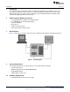
3 Block Diagram ............................................................................................................... 2
4 System Requirements ...................................................................................................... 2
4.1 Hardware Requirements .......................................................................................... 2
5 Serial Interface and Programming Connectors ......................................................................... 3
5.1 Serial Interface “J” ................................................................................................. 3
5.2 Electrical Characteristics of I
2
C .................................................................................. 4
6 I
2
C Compatible Interface ................................................................................................... 4
6.1 I
2
C Signals .......................................................................................................... 4
6.2 I
2
C Data Validity .................................................................................................... 4
6.3 I
2
C Start and Stop Conditions .................................................................................... 4
6.4 Transferring Data .................................................................................................. 5
List of Figures
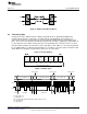
1 Block Diagram............................................................................................................... 2
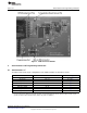
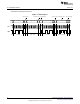
2 USB I
2
C Interface Module.................................................................................................. 3
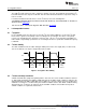
3 I
2
C Signals: Data Validity................................................................................................... 4
4 START and STOP Conditions............................................................................................. 5
5 I
2
C Chip Address............................................................................................................ 5
6 I
2
C Write Cycle .............................................................................................................. 5
7 I
2
C Read Cycle .............................................................................................................. 6
All trademarks are the property of their respective owners.
1
SNVA343A–April 2008–Revised April 2013
AN-1840 USB I
2
C Interface Board Reference Manual
Submit Documentation Feedback
Copyright © 2008–2013, Texas Instruments Incorporated