INA219 SBOS448F – AUGUST 2008 – REVISED SEPTEMBER 2011 www.ti.com Zerø-Drift, Bi-Directional CURRENT/POWER MONITOR with I2C™ Interface Check for Samples: INA219 FEATURES DESCRIPTION • • • • The INA219 is a high-side current shunt and power monitor with an I2C interface. The INA219 monitors both shunt drop and supply voltage, with programmable conversion times and filtering. A programmable calibration value, combined with an internal multiplier, enables direct readouts in amperes.
INA219 SBOS448F – AUGUST 2008 – REVISED SEPTEMBER 2011 www.ti.com This integrated circuit can be damaged by ESD. Texas Instruments recommends that all integrated circuits be handled with appropriate precautions. Failure to observe proper handling and installation procedures can cause damage. ESD damage can range from subtle performance degradation to complete device failure.
INA219 SBOS448F – AUGUST 2008 – REVISED SEPTEMBER 2011 www.ti.com ELECTRICAL CHARACTERISTICS: VS = +3.3V Boldface limits apply over the specified temperature range, TA = –25°C to +85°C. At TA = +25°C, VIN+ = 12V, VSENSE = (VIN+ – VIN–) = 32mV, PGA = ÷ 1, and BRNG (1) = 1, unless otherwise noted.
INA219 SBOS448F – AUGUST 2008 – REVISED SEPTEMBER 2011 www.ti.com ELECTRICAL CHARACTERISTICS: VS = +3.3V (continued) Boldface limits apply over the specified temperature range, TA = –25°C to +85°C. At TA = +25°C, VIN+ = 12V, VSENSE = (VIN+ – VIN–) = 32mV, PGA = ÷ 1, and BRNG(1) = 1, unless otherwise noted. INA219A PARAMETER TEST CONDITIONS MIN INA219B TYP MAX 28 MIN TYP MAX UNIT 35 28 35 ms 1 0.
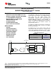
INA219 SBOS448F – AUGUST 2008 – REVISED SEPTEMBER 2011 www.ti.com PIN CONFIGURATIONS DCN PACKAGE SOT23-8 (Top View) D PACKAGE SO-8 (Top View) VIN+ 1 8 A1 VIN- 2 7 A0 GND 3 6 SDA VS 4 5 SCL A1 1 8 VIN+ A0 2 7 VIN- SDA 3 6 GND SCL 4 5 VS PIN DESCRIPTIONS: SOT23-8 SOT23-8 (DCN) PIN NO NAME 1 VIN+ Positive differential shunt voltage. Connect to positive side of shunt resistor. DESCRIPTION 2 VIN– Negative differential shunt voltage.
INA219 SBOS448F – AUGUST 2008 – REVISED SEPTEMBER 2011 www.ti.com TYPICAL CHARACTERISTICS At TA = +25°C, VIN+ = 12V, VSENSE = (VIN+ – VIN–) = 32mV, PGA = ÷ 1, and BRNG = 1, unless otherwise noted.
INA219 SBOS448F – AUGUST 2008 – REVISED SEPTEMBER 2011 www.ti.com TYPICAL CHARACTERISTICS (continued) At TA = +25°C, VIN+ = 12V, VSENSE = (VIN+ – VIN–) = 32mV, PGA = ÷ 1, and BRNG = 1, unless otherwise noted. INPUT CURRENTS WITH LARGE DIFFERENTIAL VOLTAGES (VIN+ at 12V, Sweep of VIN–) 2.0 ACTIVE IQ vs TEMPERATURE 1.2 VS+ = 5V 1.0 1.0 VS = 5V 0.8 0.5 IQ (mA) Input Currents (mA) 1.5 VS+ = 3V 0 VS+ = 3V 0.6 VS = 3V 0.4 -0.5 0.2 -1.0 VS+ = 5V 0 -1.
INA219 SBOS448F – AUGUST 2008 – REVISED SEPTEMBER 2011 www.ti.com REGISTER BLOCK DIAGRAM Power (1) Bus Voltage (1) ´ Shunt Voltage Channel Current (1) ADC Bus Voltage Channel Full-Scale Calibration (2) ´ Shunt Voltage (1) PGA (In Configuration Register) NOTES: (1) Read-only (2) Read/write Data Registers Figure 12.
INA219 SBOS448F – AUGUST 2008 – REVISED SEPTEMBER 2011 www.ti.com APPLICATION INFORMATION The INA219 is a digital current-shunt monitor with an I2C and SMBus-compatible interface. It provides digital current, voltage, and power readings necessary for accurate decision-making in precisely-controlled systems. Programmable registers allow flexible configuration for measurement resolution, and continuousversus-triggered operation.
INA219 SBOS448F – AUGUST 2008 – REVISED SEPTEMBER 2011 www.ti.com Serial Bus Address WRITING TO/READING FROM THE INA219 To communicate with the INA219, the master must first address slave devices via a slave address byte. The slave address byte consists of seven address bits, and a direction bit indicating the intent of executing a read or write operation. Accessing a particular register on the INA219 is accomplished by writing the appropriate value to the register pointer.
INA219 SBOS448F – AUGUST 2008 – REVISED SEPTEMBER 2011 www.ti.
INA219 SBOS448F – AUGUST 2008 – REVISED SEPTEMBER 2011 www.ti.com ALERT 1 9 1 9 SCL SDA 0 0 0 1 1 0 0 1 R/W Start By Master 0 0 A3 A2 ACK By INA219 A1 A0 0 From INA219 Frame 1 SMBus ALERT Response Address Byte Frame 2 Slave Address Byte NACK By Master Stop By Master (1) NOTE (1): The value of the Slave Address Byte is determined by the settings of the A0 and A1 pins. Refer to Table 1. Figure 16.
INA219 SBOS448F – AUGUST 2008 – REVISED SEPTEMBER 2011 www.ti.com High-Speed I2C Mode The master then generates a repeated start condition (a repeated start condition has the same timing as the start condition). After this repeated start condition, the protocol is the same as F/S mode, except that transmission speeds up to 3.4Mbps are allowed. Instead of using a stop condition, repeated start conditions should be used to secure the bus in HS-mode.
INA219 SBOS448F – AUGUST 2008 – REVISED SEPTEMBER 2011 www.ti.com Power-Up Conditions (Configuration Register, BADC bits). The Mode control in the Configuration Register also permits selecting modes to convert only voltage or current, either continuously or in response to an event (triggered). Power-up conditions apply to a software reset via the RST bit (bit 15) in the Configuration Register, or the I2C bus General Call Reset.
INA219 SBOS448F – AUGUST 2008 – REVISED SEPTEMBER 2011 www.ti.com Although the INA219 can be read at any time, and the data from the last conversion remain available, the Conversion Ready bit (Status Register, CNVR bit) is provided to help co-ordinate one-shot or triggered conversions. The Conversion Ready bit is set after all conversions, averaging, and multiplication operations are complete. The Conversion Ready bit clears under these conditions: 1.
INA219 SBOS448F – AUGUST 2008 – REVISED SEPTEMBER 2011 www.ti.com Overload conditions are another consideration for the INA219 inputs. The INA219 inputs are specified to tolerate 26V across the inputs. A large differential scenario might be a short to ground on the load side of the shunt. This type of event can result in full power-supply voltage across the shunt (as long the power supply or energy storage capacitors support it).
INA219 SBOS448F – AUGUST 2008 – REVISED SEPTEMBER 2011 www.ti.com PROGRAMMING THE INA219 POWER MEASUREMENT ENGINE Calibration Register and Scaling The Calibration Register makes it possible to set the scaling of the Current and Power Registers to whatever values are most useful for a given application.
INA219 SBOS448F – AUGUST 2008 – REVISED SEPTEMBER 2011 www.ti.com 6. Calculate the Power LSB, using Equation 5. Equation 5 shows a general formula; because the bus voltage measurement LSB is always 4mV, the power formula reduces to the calculated result. Power_LSB = 20 Current_LSB Power_LSB = 400 ´ 10-6 (5) 7. Compute the maximum current and shunt voltage values (before overflow), as shown by Equation 6 and Equation 7.
INA219 SBOS448F – AUGUST 2008 – REVISED SEPTEMBER 2011 www.ti.com Figure 21 illustrates how to perform the same procedure discussed in this example using the automated INA219EVM software. Note that the same numbers used in the nine-step example are used in the software example in Figure 21. Also note that Figure 21 illustrates which results correspond to which step (for example, the information entered in Step 1 is enclosed in a box in Figure 21 and labeled).
INA219 SBOS448F – AUGUST 2008 – REVISED SEPTEMBER 2011 www.ti.com Calibration Example 2 (Overflow Possible) This design example uses the nine-step procedure for calibrating the INA219 where overflow is possible. Figure 22 illustrates how the same procedure is performed using the automated INA219EVM software. Note that the same numbers used in the nine-step example are used in the software example in Figure 22.
INA219 SBOS448F – AUGUST 2008 – REVISED SEPTEMBER 2011 www.ti.com 7. Compute the maximum current and shunt voltage values (before overflow), as shown by Equation 15 and Equation 16. Note that both Equation 15 and Equation 16 involve an If - then condition. Max_Current = Current_LSB ´ 32767 Max_Current = 0.
INA219 SBOS448F – AUGUST 2008 – REVISED SEPTEMBER 2011 www.ti.com Figure 22 illustrates how to perform the same procedure discussed in this example using the automated INA219EVM software. Note that the same numbers used in the nine-step example are used in the software example in Figure 22. Also note that Figure 22 illustrates which results correspond to which step (for example, the information entered in Step 1 is enclosed in a box in Figure 22 and labeled).
INA219 SBOS448F – AUGUST 2008 – REVISED SEPTEMBER 2011 www.ti.com CONFIGURE/MEASURE/CALCULATE EXAMPLE shunt voltage. By knowing the value of the shunt resistor, the device can then calculate the amount of current that created the measured shunt voltage drop. The first step when calculating the calibration value is setting the current LSB. The Calibration Register value is based on a calculation that has its precision capability limited by the size of the register and the Current Register LSB.
INA219 SBOS448F – AUGUST 2008 – REVISED SEPTEMBER 2011 www.ti.com The Current Register (04h) is then calculated by multiplying the shunt voltage contents by the Calibration Register and then dividing by 4096. For this example, the shunt voltage of 2000 is multiplied by the calibration register of 20480 and then divided by 4096 to yield a Current Register of 2710h.
INA219 SBOS448F – AUGUST 2008 – REVISED SEPTEMBER 2011 www.ti.com REGISTER INFORMATION The INA219 uses a bank of registers for holding configuration settings, measurement results, maximum/minimum limits, and status information. Table 4 summarizes the INA219 registers; Figure 12 illustrates registers. Register contents are updated 4μs after completion of the write command.
INA219 SBOS448F – AUGUST 2008 – REVISED SEPTEMBER 2011 www.ti.com REGISTER DETAILS All INA219 registers 16-bit registers are actually two 8-bit bytes via the I2C interface.
INA219 SBOS448F – AUGUST 2008 – REVISED SEPTEMBER 2011 www.ti.com SADC: SADC Shunt ADC Resolution/Averaging Bits 3–6 These bits adjust the Shunt ADC resolution (9-, 10-, 11-, or 12-bit) or set the number of samples used when averaging results for the Shunt Voltage Register (01h). BADC (Bus) and SADC (Shunt) ADC resolution/averaging and conversion time settings are shown in Table 6. Table 6.
INA219 SBOS448F – AUGUST 2008 – REVISED SEPTEMBER 2011 www.ti.com DATA OUTPUT REGISTERS Shunt Voltage Register 01h (Read-Only) The Shunt Voltage Register stores the current shunt voltage reading, VSHUNT. Shunt Voltage Register bits are shifted according to the PGA setting selected in the Configuration Register (00h). When multiple sign bits are present, they will all be the same value. Negative numbers are represented in two's complement format.
INA219 SBOS448F – AUGUST 2008 – REVISED SEPTEMBER 2011 www.ti.com Table 8. Shunt Voltage Register Format (1) VSHUNT Reading (mV) Decimal Value PGA = ÷ 8 (D15…..................D0) PGA = ÷ 4 (D15…..................D0) PGA = ÷ 2 (D15…..................D0) PGA = ÷ 1 (D15…..................D0) 320.02 32002 0111 1101 0000 0000 0011 1110 1000 0000 0001 1111 0100 0000 0000 1111 1010 0000 320.01 32001 0111 1101 0000 0000 0011 1110 1000 0000 0001 1111 0100 0000 0000 1111 1010 0000 320.
INA219 SBOS448F – AUGUST 2008 – REVISED SEPTEMBER 2011 www.ti.com Bus Voltage Register 02h (Read-Only) The Bus Voltage Register stores the most recent bus voltage reading, VBUS. At full-scale range = 32V (decimal = 8000, hex = 1F40), and LSB = 4mV.
INA219 SBOS448F – AUGUST 2008 – REVISED SEPTEMBER 2011 www.ti.com CALIBRATION REGISTER Calibration Register 05h (Read/Write) Current and power calibration are set by bits D15 to D1 of the Calibration Register. Note that bit D0 is not used in the calculation. This register sets the current that corresponds to a full-scale drop across the shunt. Full-scale range and the LSB of the current and power measurement depend on the value entered in this register.
PACKAGE OPTION ADDENDUM www.ti.
PACKAGE OPTION ADDENDUM www.ti.com (3) 19-Apr-2013 MSL, Peak Temp. -- The Moisture Sensitivity Level rating according to the JEDEC industry standard classifications, and peak solder temperature. (4) Multiple Top-Side Markings will be inside parentheses. Only one Top-Side Marking contained in parentheses and separated by a "~" will appear on a device. If a line is indented then it is a continuation of the previous line and the two combined represent the entire Top-Side Marking for that device.
PACKAGE MATERIALS INFORMATION www.ti.com 21-Sep-2011 TAPE AND REEL INFORMATION *All dimensions are nominal Device Package Package Pins Type Drawing SPQ Reel Reel A0 Diameter Width (mm) (mm) W1 (mm) INA219AIDCNR SOT-23 DCN 8 3000 179.0 8.4 B0 (mm) K0 (mm) P1 (mm) W Pin1 (mm) Quadrant 3.2 3.2 1.4 4.0 8.0 Q3 INA219AIDCNT SOT-23 DCN 8 250 179.0 8.4 3.2 3.2 1.4 4.0 8.0 Q3 INA219BIDCNR SOT-23 DCN 8 3000 179.0 8.4 3.2 3.2 1.4 4.0 8.
PACKAGE MATERIALS INFORMATION www.ti.com 21-Sep-2011 *All dimensions are nominal Device Package Type Package Drawing Pins SPQ Length (mm) Width (mm) Height (mm) INA219AIDCNR SOT-23 DCN 8 3000 195.0 200.0 45.0 INA219AIDCNT SOT-23 DCN 8 250 195.0 200.0 45.0 INA219BIDCNR SOT-23 DCN 8 3000 195.0 200.0 45.0 INA219BIDCNT SOT-23 DCN 8 250 195.0 200.0 45.
IMPORTANT NOTICE Texas Instruments Incorporated and its subsidiaries (TI) reserve the right to make corrections, enhancements, improvements and other changes to its semiconductor products and services per JESD46, latest issue, and to discontinue any product or service per JESD48, latest issue. Buyers should obtain the latest relevant information before placing orders and should verify that such information is current and complete.