INA INA282, INA283 INA284, INA285 INA286 28x www.ti.
INA282, INA283 INA284, INA285 INA286 SBOS485B – NOVEMBER 2009 – REVISED SEPTEMBER 2012 www.ti.com This integrated circuit can be damaged by ESD. Texas Instruments recommends that all integrated circuits be handled with appropriate precautions. Failure to observe proper handling and installation procedures can cause damage. ESD damage can range from subtle performance degradation to complete device failure.
INA282, INA283 INA284, INA285 INA286 www.ti.com SBOS485B – NOVEMBER 2009 – REVISED SEPTEMBER 2012 ELECTRICAL CHARACTERISTICS Boldface limits apply over the specified temperature range, TA = –40°C to +125°C. At TA = +25°C, V+ = 5V, V+IN = 12V, VREF1 = VREF2 = 2.048V referenced to GND, and VSENSE = V+IN – V–IN, unless otherwise noted.
INA282, INA283 INA284, INA285 INA286 SBOS485B – NOVEMBER 2009 – REVISED SEPTEMBER 2012 www.ti.com ELECTRICAL CHARACTERISTICS (continued) Boldface limits apply over the specified temperature range, TA = –40°C to +125°C. At TA = +25°C, V+ = 5V, V+IN = 12V, VREF1 = VREF2 = 2.048V referenced to GND, and VSENSE = V+IN – V–IN, unless otherwise noted. INA282, INA283, INA284, INA285, INA286 PARAMETER CONDITIONS VOLTAGE OUTPUT (6) MIN TYP MAX UNIT (V+)–0.17 (V+)–0.4 V GND+0.015 GND+0.
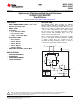
INA282, INA283 INA284, INA285 INA286 www.ti.com SBOS485B – NOVEMBER 2009 – REVISED SEPTEMBER 2012 PIN CONFIGURATION D PACKAGE SOIC-8 (TOP VIEW) -IN 1 8 +IN GND 2 7 REF1 REF2 3 6 V+ (1) 4 5 OUT NC (1) NC: This pin is not internally connected. The NC pin should either be left floating or connected to GND. PIN DESCRIPTIONS SOIC-8 PIN NO. NAME DESCRIPTION 1 –IN 2 GND Connection to negative side of shunt resistor.
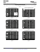
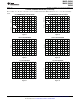
INA282, INA283 INA284, INA285 INA286 SBOS485B – NOVEMBER 2009 – REVISED SEPTEMBER 2012 www.ti.com TYPICAL CHARACTERISTICS At TA = +25°C, V+ = 5V, V+IN = 12V, VREF1 = VREF2 = 2.048V referenced to GND, and VSENSE = V+IN – V–IN, unless otherwise noted. START-UP TRANSIENT RESPONSE START-UP TRANSIENT RESPONSE VREF = GND, VDRIVE = 0.125V, RLOAD = 10kW, CLOAD = 10pF CLOAD = 10pF VREF = GND VDRIVE = 0.125V RLOAD = 10kW 5V/div V+ V+ 25ms/div 250ms/div Figure 1. Figure 2.
INA282, INA283 INA284, INA285 INA286 www.ti.com SBOS485B – NOVEMBER 2009 – REVISED SEPTEMBER 2012 TYPICAL CHARACTERISTICS (continued) At TA = +25°C, V+ = 5V, V+IN = 12V, VREF1 = VREF2 = 2.048V referenced to GND, and VSENSE = V+IN – V–IN, unless otherwise noted. VOUT VCM 10V/div 500mV/div VOUT 10V/div 50V COMMON-MODE STEP RESPONSE 500mV/div 50V COMMON-MODE STEP RESPONSE VCM 5ms/div 5ms/div Figure 8. 100mV STEP RESPONSE 500mV STEP RESPONSE 20mV/div 100mV/div Figure 7. 10ms/div Figure 9.
INA282, INA283 INA284, INA285 INA286 SBOS485B – NOVEMBER 2009 – REVISED SEPTEMBER 2012 www.ti.com TYPICAL CHARACTERISTICS (continued) At TA = +25°C, V+ = 5V, V+IN = 12V, VREF1 = VREF2 = 2.048V referenced to GND, and VSENSE = V+IN – V–IN, unless otherwise noted. INA282 PSRR (RTI) vs FREQUENCY INPUT OVERLOAD 120 Power-Supply Rejection Ratio (dB) Input Drive (1V to 0V) 1V/div VOUT (5V to midsupply) 110 100 90 80 70 60 50 40 30 20 25ms/div 100 1k 10k 100k 1M Frequency (Hz) Figure 13. Figure 14.
INA282, INA283 INA284, INA285 INA286 www.ti.com SBOS485B – NOVEMBER 2009 – REVISED SEPTEMBER 2012 TYPICAL CHARACTERISTICS (continued) At TA = +25°C, V+ = 5V, V+IN = 12V, VREF1 = VREF2 = 2.048V referenced to GND, and VSENSE = V+IN – V–IN, unless otherwise noted. INA282 TYPICAL NONLINEARITY vs OUTPUT VOLTAGE INA283 +IN BIAS CURRENT vs COMMON-MODE VOLTAGE 30 0.06 VSENSE = -50mV to +50mV 20 +IN Bias Current (mA) Nonlinearity (%) 0.04 0.02 0 V+ = 18V -0.02 V+ = 3.5V -0.04 V+ = 18V 0 -10 -20 -30 -40 -0.
INA282, INA283 INA284, INA285 INA286 SBOS485B – NOVEMBER 2009 – REVISED SEPTEMBER 2012 www.ti.com TYPICAL CHARACTERISTICS (continued) At TA = +25°C, V+ = 5V, V+IN = 12V, VREF1 = VREF2 = 2.048V referenced to GND, and VSENSE = V+IN – V–IN, unless otherwise noted. +IN BIAS CURRENT vs TEMPERATURE GAIN vs TEMPERATURE 1.0 0 0.8 -5 0.4 +IN Bias Current (mA) Deviation in Gain (%) 0.6 V+ = 5V 0.2 0 -0.2 V+ = 12V -0.4 -0.6 -10 V+ = 2.7V -15 -20 V+ = 5V -25 V+ = 18V -30 -0.8 -35 -1.
INA282, INA283 INA284, INA285 INA286 www.ti.com SBOS485B – NOVEMBER 2009 – REVISED SEPTEMBER 2012 TYPICAL CHARACTERISTICS (continued) At TA = +25°C, V+ = 5V, V+IN = 12V, VREF1 = VREF2 = 2.048V referenced to GND, and VSENSE = V+IN – V–IN, unless otherwise noted. INA283 SWING TO GROUND vs OUTPUT CURRENT 400 Swing to Ground (mV) 350 300 250 +125°C 200 150 100 2.7V Swing 5V Swing 18V Swing +85°C 50 +25°C 0 0 0.5 -40°C 1.0 1.5 2.0 2.5 IOUT, Sinking (mA) Figure 31.
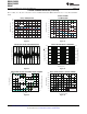
INA282, INA283 INA284, INA285 INA286 SBOS485B – NOVEMBER 2009 – REVISED SEPTEMBER 2012 www.ti.com APPLICATIONS INFORMATION GENERAL INFORMATION The INA282 family voltage output current shunt monitors feature a common-mode range that extends 14V below the negative supply rail, as well as up to 80V, which allows use for either low-side or high-side current sensing. BASIC CONNECTIONS Figure 32 shows the basic connection of an INA282 family device.
INA282, INA283 INA284, INA285 INA286 www.ti.com SBOS485B – NOVEMBER 2009 – REVISED SEPTEMBER 2012 POWER SUPPLY The INA282 family can make accurate measurements well outside of its own power-supply voltage, V+, because its inputs (+IN and –IN) may operate anywhere between –14V and +80V independent of V+. For example, the V+ power supply can be 5V while the common-mode voltage being monitored by the shunt may be as high as +80V.
INA282, INA283 INA284, INA285 INA286 SBOS485B – NOVEMBER 2009 – REVISED SEPTEMBER 2012 www.ti.com REFERENCE PIN CONNECTION OPTIONS Figure 33 illustrates a test circuit for reference divider accuracy. The output of the INA282 family can be connected for unidirectional or bidirectional operation. Note that neither the REF1 pin nor the REF2 pin may be connected to any voltage source lower than GND or higher than V+, and that the effective reference voltage (REF1 + REF2)/2 must be 9V or less.
INA282, INA283 INA284, INA285 INA286 www.ti.com SBOS485B – NOVEMBER 2009 – REVISED SEPTEMBER 2012 UNIDIRECTIONAL OPERATION Unidirectional operation allows the INA282 family to measure currents through a resistive shunt in one direction. In the case of unidirectional operation, the output could be set at the negative rail (near ground, and the most common connection) or at the positive rail (near V+) when the differential input is 0V.
INA282, INA283 INA284, INA285 INA286 SBOS485B – NOVEMBER 2009 – REVISED SEPTEMBER 2012 www.ti.com V+ Referenced Output This mode is set when both reference pins are connected to the positive supply. It is typically used when a diagnostic scheme requires detection of the amplifier and the wiring before power is applied to the load (as shown in Figure 35).
INA282, INA283 INA284, INA285 INA286 www.ti.com SBOS485B – NOVEMBER 2009 – REVISED SEPTEMBER 2012 BIDIRECTIONAL OPERATION Bidirectional operation allows the INA282 family to measure currents through a resistive shunt in two directions. In this case, the output can be set anywhere within the limits of what the reference inputs allow (that is, between 0V to 9V, but never to exceed the supply voltage). Typically, it is set at half-scale for equal range in both directions.
INA282, INA283 INA284, INA285 INA286 SBOS485B – NOVEMBER 2009 – REVISED SEPTEMBER 2012 www.ti.com Splitting the Supply By connecting one reference pin to V+ and the other to the ground pin, the output is set at half of the supply when there is no differential input, as shown in Figure 37. This method creates a midscale offset that is ratiometric to the supply voltage; thus, if the supply increases or decreases, the output remains at half the supply.
INA282, INA283 INA284, INA285 INA286 www.ti.com SBOS485B – NOVEMBER 2009 – REVISED SEPTEMBER 2012 Splitting an External Reference In this case, an external reference is divided by 2 with an accuracy of approximately 0.5% by connecting one REF pin to ground and the other REF pin to the reference (as Figure 38 illustrates). Supply -14V to +80V Load V+ +IN Æ1 V+ -IN Æ2 Æ2 Æ2 Æ1 Æ2 Æ1 Æ1 OUT ZerÆDrift GAIN PRODUCT 50V/V 100V/V 200V/V 500V/V 1000V/V INA282 INA286 INA283 INA284 INA285 33.
INA282, INA283 INA284, INA285 INA286 SBOS485B – NOVEMBER 2009 – REVISED SEPTEMBER 2012 www.ti.com EXTENDED NEGATIVE COMMON-MODE RANGE Using a negative power supply can extend the common-mode range 14V more negative than the supply used. For instance, a –10V supply allows up to –24V negative common-mode. Remember to keep the total voltage between the GND pin and V+ pin to less than 18V. The positive common-mode decreases by the same amount.
INA282, INA283 INA284, INA285 INA286 www.ti.com SBOS485B – NOVEMBER 2009 – REVISED SEPTEMBER 2012 The nonlinearity error of the INA282-286 is relatively low compared to the gain error specification, which results in a gain error that can be expected to be relatively constant throughout the linear input range of the device. While the gain error remains constant across the linear input range of the device, the error associated with the input offset voltage does not.
INA282, INA283 INA284, INA285 INA286 SBOS485B – NOVEMBER 2009 – REVISED SEPTEMBER 2012 www.ti.com Example 2 INA286; VS = 5V; VCM = 24V; VREF = 0V; VSENSE = 10mV Table 2. Example 2 TERM SYMBOL EQUATION TYPICAL VALUE MAXIMUM VALUE Initial Input Offset Voltage VOS — 20μV 70μV Added Input Offset Voltage Because of Common-Mode Voltage VOS_CM 1.2μV 12μV Added Input Offset Voltage Because of Reference Voltage VOS_REF 34.8μV 92.
INA282, INA283 INA284, INA285 INA286 www.ti.com SBOS485B – NOVEMBER 2009 – REVISED SEPTEMBER 2012 CURRENT DIFFERENCING Occasionally, the need arises to confirm that the current into a load is identical to the current out of a load, usually as part of diagnostic testing or fault detection. This situation requires precision current differencing, which is the same as summing except that the two amplifiers have the inputs connected opposite of each other.
INA282, INA283 INA284, INA285 INA286 SBOS485B – NOVEMBER 2009 – REVISED SEPTEMBER 2012 www.ti.com COMMON-MODE DYNAMICS AND CURRENT DIFFERENCING Current sensing is frequently used on totem-pole output stages, such as those of bridge-type motor drives. We can sense current in one of three locations on a totem-pole output: on the ground side (low-side sensing); on the power-supply side (high-side sensing); or on the output (phase sensing). Only the output line reports the exact load current.
INA282, INA283 INA284, INA285 INA286 www.ti.com SBOS485B – NOVEMBER 2009 – REVISED SEPTEMBER 2012 Æ2 +2.7V to +18V Æ2 Æ2 Æ1 VIN+ Æ1 Æ1 VIN- Æ2 Æ1 Motor Supply (< 80V) Q1 D1 MOSFET Drive Circuits VREF Output +2.7V to +18V Æ2 Æ2 Æ1 VIN+ Æ1 Æ1 VIN- Æ2 Æ1 Q2 Æ2 D2 NOTE: By sensing totem-pole current on both the positive and negative rail and summing, dynamic common-mode issues can be avoided entirely.
INA282, INA283 INA284, INA285 INA286 SBOS485B – NOVEMBER 2009 – REVISED SEPTEMBER 2012 www.ti.com Changes from Revision A (July 2010) to Revision B • 26 Page Changed devices from product preview to production data. ................................................................................................
PACKAGE OPTION ADDENDUM www.ti.
PACKAGE OPTION ADDENDUM www.ti.com 12-Feb-2014 (3) MSL, Peak Temp. - The Moisture Sensitivity Level rating according to the JEDEC industry standard classifications, and peak solder temperature. (4) There may be additional marking, which relates to the logo, the lot trace code information, or the environmental category on the device. (5) Multiple Device Markings will be inside parentheses. Only one Device Marking contained in parentheses and separated by a "~" will appear on a device.
PACKAGE MATERIALS INFORMATION www.ti.com 14-Mar-2013 TAPE AND REEL INFORMATION *All dimensions are nominal Device Package Package Pins Type Drawing SPQ Reel Reel A0 Diameter Width (mm) (mm) W1 (mm) B0 (mm) K0 (mm) P1 (mm) W Pin1 (mm) Quadrant INA282AIDR SOIC D 8 2500 330.0 12.4 6.4 5.2 2.1 8.0 12.0 Q1 INA283AIDR SOIC D 8 2500 330.0 12.4 6.4 5.2 2.1 8.0 12.0 Q1 INA285AIDR SOIC D 8 2500 330.0 12.4 6.4 5.2 2.1 8.0 12.0 Q1 INA286AIDR SOIC D 8 2500 330.
PACKAGE MATERIALS INFORMATION www.ti.com 14-Mar-2013 *All dimensions are nominal Device Package Type Package Drawing Pins SPQ Length (mm) Width (mm) Height (mm) INA282AIDR SOIC D 8 2500 367.0 367.0 35.0 INA283AIDR SOIC D 8 2500 367.0 367.0 35.0 INA285AIDR SOIC D 8 2500 367.0 367.0 35.0 INA286AIDR SOIC D 8 2500 367.0 367.0 35.
IMPORTANT NOTICE Texas Instruments Incorporated and its subsidiaries (TI) reserve the right to make corrections, enhancements, improvements and other changes to its semiconductor products and services per JESD46, latest issue, and to discontinue any product or service per JESD48, latest issue. Buyers should obtain the latest relevant information before placing orders and should verify that such information is current and complete.