
Datasheet

LM1085
www.ti.com
SNVS038G –JULY 1999–REVISED MARCH 2013
These devices have limited built-in ESD protection. The leads should be shorted together or the device placed in conductive foam
during storage or handling to prevent electrostatic damage to the MOS gates.
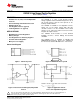
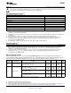
Absolute Maximum Ratings
(1)(2)
Maximum Input to Output Voltage Differential
LM1085-ADJ 29V
LM1085-12 18V
LM1085-3.3 27V
LM1085-5.0 25V
Power Dissipation
(3)
Internally Limited
Junction Temperature (T
J
)
(4)
150°C
Storage Temperature Range -65°C to 150°C
Lead Temperature 260°C, to 10 sec
ESD Tolerance
(5)
2000V
(1) Absolute Maximum Ratings indicate limits beyond which damage to the device may occur. Operating Ratings indicate conditions for
which the device is intended to be functional, but specific performance is not ensured. For ensured specifications and the test
conditions, see the Electrical Characteristics.
(2) If Military/Aerospace specified devices are required, please contact the Texas Instruments Sales Office/ Distributors for availability and
specifications.
(3) Power dissipation is kept in a safe range by current limiting circuitry. Refer to Overload Recovery in Application Notes.
(4) The maximum power dissipation is a function of T
J(max)
, θ
JA
, and T
A
. The maximum allowable power dissipation at any ambient
temperature is P
D
= (T
J(max)
–T
A
)/θ
JA
. All numbers apply for packages soldered directly into a PC board. Refer to Thermal
Considerations in the Application Notes.
(5) For testing purposes, ESD was applied using human body model, 1.5kΩ in series with 100pF.
Operating Ratings
(1)
Junction Temperature (T
J
)
(2)
−40°C to 125°C
(1) Absolute Maximum Ratings indicate limits beyond which damage to the device may occur. Operating Ratings indicate conditions for
which the device is intended to be functional, but specific performance is not ensured. For ensured specifications and the test
conditions, see the Electrical Characteristics.
(2) The maximum power dissipation is a function of T
J(max)
, θ
JA
, and T
A
. The maximum allowable power dissipation at any ambient
temperature is P
D
= (T
J(max)
–T
A
)/θ
JA
. All numbers apply for packages soldered directly into a PC board. Refer to Thermal
Considerations in the Application Notes.
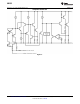
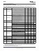
Electrical Characteristics
Limits in standard type are for T
J
= 25°C only; limits in boldface type apply over the operating junction temperature (T
J
)
range of -40°C to +125°C. Minimum and Maximum limits are ensured through test, design, or statistical correlation. Typical
values represent the most likely parametric norm at T
J
= 25°C, and are provided for reference purposes only.
Min Typ Max
Symbol Parameter Conditions Units
(1) (2) (1)
LM1085-ADJ
Reference Voltage
V
REF
I
OUT
= 10mA, V
IN
−V
OUT
= 3V 1.238 1.250 1.262 V
(3)
10mA ≤I
OUT
≤ I
FULL LOAD
,1.5V ≤ (V
IN
−V
OUT
) ≤ 15V 1.225 1.250 1.270
LM1085-3.3
I
OUT
= 0mA, V
IN
= 5V 3.270 3.300 3.330 V
0 ≤ I
OUT
≤I
FULL LOAD
, 4.8V≤ V
IN
≤15V 3.235 3.300 3.365
LM1085-5.0
Output Voltage
V
OUT
I
OUT
= 0mA, V
IN
= 8V 4.950 5.000 5.050 V
(3)
0 ≤ I
OUT
≤ I
FULL LOAD
, 6.5V ≤ V
IN
≤ 20V 4.900 5.000 5.100
LM1085-12
I
OUT
= 0mA, V
IN
= 15V 11.880 12.000 12.120 V
0 ≤ I
OUT
≤ I
FULL LOAD
, 13.5V ≤ V
IN
≤ 25V 11.760 12.000 12.240
(1) All limits are specified by testing or statistical analysis.
(2) Typical Values represent the most likely parametric norm.
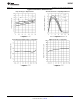
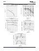
(3) I
FULL LOAD
is defined in the current limit curves. The I
FULL LOAD
Curve defines the current limit as a function of input-to-output voltage.
Note that 30W power dissipation for the LM1085 is only achievable over a limited range of input-to-output voltage.
Copyright © 1999–2013, Texas Instruments Incorporated Submit Documentation Feedback 3
Product Folder Links: LM1085